Open-Photonics · Si · SiN · TFLN · BTO · InP
Silicon Photonics and Lasers, from Waveguides to Tested Chips
An open, interactive tutorial on integrated photonics: electromagnetic theory and Gaussian beams, waveguides on SOI, passive devices, coupling to fibre, modulators and detectors, lasers from first principles to lasers on silicon, and the fabrication, testing and data analysis that turn a layout into a working chip.
Start reading See the course map PDK devices in 3D Source on GitHub
A photonic integrated circuit does with light what an electronic chip does with charge: it generates, routes, filters, modulates and detects signals, on a wafer, in volume. This tutorial builds that picture from the ground up. Every concept follows the same pattern: a short derivation, a worked example with real numbers, an interactive demo you can play with, and a what this means for your design box. Where the open process design kits allow it, you can turn the real device over in 3D.
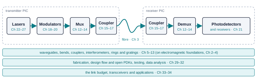
What is inside
Foundations
Why integrated photonics, electromagnetic theory, Gaussian beams and fibres, and the Si, SiN, TFLN, BTO and InP platforms.
Waveguides
Slab and channel waveguides on SOI and other platforms, loss and dispersion, bends, tapers and transitions.
Passive devices
Directional couplers, Y-branches and MMIs, Mach–Zehnder interferometers, rings, Bragg gratings, WDM and polarisation devices.
Coupling and packaging
Grating and edge couplers, fibre arrays, photonic wire bonds and packaging.
Active devices
Thermo-optic tuning, electro-optic effects in each platform, modulators, photodetectors and receivers.
Lasers and amplifiers
Gain from first principles, the Fabry–Pérot laser and its rate equations, noise and linewidth, tunable lasers, lasers on silicon and SOAs.
Fabrication, testing and data
Fabrication and its variations, the design flow and open PDKs, test setups and data analysis.
Systems and applications
Optical links and transceivers, and the sensing, LiDAR, quantum and computing systems built from the same blocks.
Hands-on labs
Simulate devices with free solvers, lay out and submit an openEBL chip, analyse real measurements, and model lasers and the reference link.
PDK devices in 3D
Devices from the SiEPIC EBeam, CORNERSTONE and Luxtelligence open PDKs, with credit to their designers; plus formulas, constants, a glossary and a directory of open tools.
Interactive demos
Each chapter has one or more demos that run in the browser with no installation: a link power budget, polarisation and wave packets, a slab-waveguide mode solver, Fresnel reflection and total internal reflection, Gaussian beams and fibre coupling, fibre modes, a platform comparator, directional couplers, MMI self-imaging, Mach–Zehnder interferometers, ring resonators, Bragg gratings by transfer matrix, grating-coupler phase matching, a fibre-array alignment game, a laser rate-equation simulator and a Vernier tunable laser, with more to come. The course map lists them all. Where a free simulation by someone else already does the job well, such as the MIT and AIM Photonics Academy virtual-lab simulations, the chapter links to it.
About
The tutorial’s organisation draws on the open teaching material of the field, above all Chrostowski and Hochberg’s Silicon Photonics Design and the UBC edX course built around it, the SiEPIC openEBL design–fabrication–test cycle, the AIM Photonics Academy courses and the open PDKs of SiEPIC and gdsfactory. It cites these works and links to them; it does not copy them. Every source is on the References page.
How this tutorial is made. It is being developed with the help of AI tools, and this draft may contain mistakes. If you spot one, please open a GitHub issue, and we will correct it.
This is a living draft (v0.1, November 2026): all eight parts (Chapters 1–34) are written, with forty-two interactive demos and the 3D gallery; the hands-on labs are the next part to be written.