Chapter 6Channel Waveguides on SOI and Beyond
Real waveguides confine light in two dimensions, and their cross-section is the first design decision on every photonic chip.
- describe strip, rib, slot and subwavelength-grating waveguides;
- apply the effective-index method, and know where it fails;
- run a numerical mode solver and read its output;
- quote the effective index, group index and single-mode width of standard SOI waveguides at 1310 and 1550 nm;
- compare waveguide cross-sections on SiN, TFLN, thick SOI and InP, and estimate how fabrication errors shift them.
Which width and etch depth give single-mode, low-loss, compact routing?
6.1Geometries
Four cross-sections cover most silicon photonics:
- Strip (or wire): the silicon film etched through to the oxide, typically 500 × 220 nm at 1550 nm. Strongest confinement, tightest bends (a few micrometres), highest scattering loss.
- Rib (or ridge): a partial etch leaves a thin slab beside the waveguide, for example 90 nm of a 220 nm film. Lower lateral contrast, so the mode spreads, scatters less and tolerates width errors better, but bends must be larger. The slab also gives electrical access to the waveguide, which is why modulators and detectors use ribs (Chapters 19–21).
- Slot: two silicon rails with a narrow gap. For the mode polarised across the gap, the normal component of \(\mathbf{D}\) is continuous, so \(\mathbf{E}\) jumps by \(n_\mathrm{Si}^2/n_\mathrm{gap}^2\) and concentrates in the low-index slot: useful for sensing and for nonlinear or electro-optic claddings.
- Subwavelength grating (SWG): silicon segments with a period well below the Bragg period, which act as an artificial material whose index is set by the fill factor. Used for mode shaping, broadband couplers and sensors.
6.2The effective-index method
A rectangular waveguide has no closed-form modes, but it can be approximated by two slab problems (Chapter 5):
- Vertical slabs. Solve the slab of the core region (thickness \(t\)) for its effective index \(n_\mathrm{I}\), and the slab of the region beside it (the remaining slab \(s\) of a rib, or just cladding for a strip) for \(n_\mathrm{II}\).
- Lateral slab. Solve a slab of width \(W\) with core index \(n_\mathrm{I}\) and cladding index \(n_\mathrm{II}\). For a TE-like mode, whose electric field is horizontal, the field is normal to the lateral interfaces, so this second slab uses the TM boundary conditions; for a TM-like mode, the reverse.
The result is the effective-index method (EIM). It is fast, intuitive and surprisingly good for ribs and wide guides. For small, high-contrast strips it overestimates the effective index and underestimates the single-mode width, because it assumes the field separates into a vertical and a lateral profile, which is not true in the corners, and because the lateral slab it builds (core index 2.85 against oxide) has more contrast than the real strip. For 500 × 220 nm at 1550 nm it gives \(n_\mathrm{eff} = 2.49\) and a TE1 cut-off at about 320 nm, against 2.446 and about 450 nm from a full solver.
Try it. Change the width, thickness, etch depth and wavelength; the cross-section shows the waveguide to scale with its mode.
6.3Numerical mode solvers
For design you solve the full vectorial wave equation on the cross-section numerically. Finite-difference eigenmode (FDE) solvers discretise the cross-section on a grid; finite-element solvers use a mesh that follows the interfaces. Both return each mode’s effective index, field and polarisation. The open-source finite-element solver femwell is used for the numbers in this chapter [17]; MPB, and the eigenmode solvers built into commercial tools, do the same job.
Three habits make a mode solver trustworthy:
- Converge the mesh. Refine until the effective index stops changing in the fourth decimal; the field near the silicon corners needs the finest mesh.
- Make the domain large enough. The evanescent tails must decay before the boundary, or the boundary perturbs the mode; leaky modes need absorbing (PML) boundaries.
- Include dispersion. Use wavelength-dependent indices, and compute the group index from effective indices at neighbouring wavelengths, \(n_g = n_\mathrm{eff} - \lambda\,\Delta n_\mathrm{eff}/\Delta\lambda\).
6.4Effective and group index of SOI waveguides
Figure 6.1 shows the modes of 220 nm silicon strips in oxide against width, computed with femwell, and Table 6.1 collects the numbers for the standard waveguides.
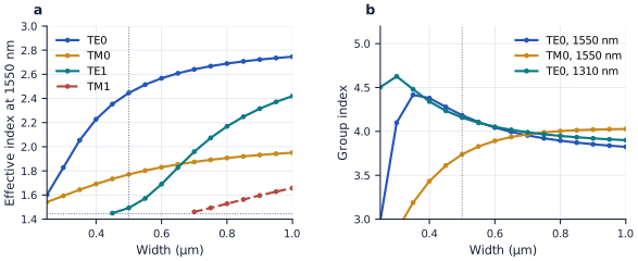
figsrc/part2_figs.py from figsrc/ch06_sweep.py.Table 6.1. Standard SOI waveguides (220 nm silicon in oxide). Full-vectorial femwell results.
| Waveguide | Wavelength | Mode | n_eff | n_g |
|---|---|---|---|---|
| Strip 500 nm | 1550 nm | TE0 | 2.446 | 4.18 |
| Strip 500 nm | 1550 nm | TM0 | 1.771 | 3.74 |
| Strip 500 nm | 1310 nm | TE0 | 2.712 | 4.16 |
| Strip 500 nm | 1310 nm | TM0 | 2.165 | 4.67 |
| Rib 500 nm, 90 nm slab | 1550 nm | TE0 | 2.568 | 3.89 |
The 500 × 220 nm strip has \(n_\mathrm{eff} = 2.446\) but \(n_g = 4.18\) at 1550 nm. Light takes \(n_gL/c = 4.18 \times 1\ \mathrm{cm}/c = 139\) ps to cross a centimetre, and an interferometer with an arm-length difference \(\Delta L\) has a free spectral range \(\lambda^2/(n_g\Delta L)\): 100 µm gives \(1.55^2/(4.18 \times 100) = 5.7\) nm (Chapter 11). Using \(n_\mathrm{eff}\) by mistake would predict 9.8 nm, a 70 % error. Whenever a spectrum’s period matters, use the group index.
6.5Single-mode conditions and polarisation
A 220 nm film is single-mode vertically at 1550 nm (Chapter 5), so the strip’s higher-order modes are lateral. At 1550 nm the second TE mode (TE1) appears at a width of about 450 nm; at 500 nm it is guided but weakly (\(n_\mathrm{eff} = 1.49\), barely above the oxide), and it is stripped by the first bend. That is why 500 nm is the usual compromise: wide enough for low scattering loss and a little tolerance, narrow enough to be effectively single-mode. At 1310 nm the same arguments give widths of about 350–400 nm.
The TE and TM modes have very different effective indices (2.45 and 1.77 at 500 nm), so the strip is strongly birefringent: TE and TM light see different phases, couplers and resonances, and grating couplers are designed for one polarisation only (Chapter 15). Where a TE and a TM mode would have equal indices, for example near widths where the curves of Figure 6.1 cross for other film thicknesses or in asymmetric claddings, they hybridise into mixed modes; polarisation rotators exploit exactly this (Chapter 14).
Route with 500 × 220 nm strips (TE, 1550 nm): \(n_\mathrm{eff} = 2.446\), \(n_g = 4.18\). Use the group index for every free spectral range and delay in Part III.
6.6Other platforms
The same tools apply to every platform; only the numbers change (Chapter 4, Figure 4.2):
- Silicon nitride. With \(n \approx 2.0\), single-mode SiN strips are around 1 µm wide and 300–800 nm thick; a 1.2 × 0.4 µm guide has an effective index of about 1.67 and an evanescent tail of about 300 nm, three times longer than silicon’s.
- Thick SOI. In 3 µm silicon, rib waveguides of a few micrometres are single-mode because their shallow etch makes the higher-order lateral modes leak into the slab; the mode is large, fibre-friendly and almost polarisation-independent [20].
- Thin-film lithium niobate. Ridges etched halfway into a 300–600 nm film guide modes that overlap the electro-optic film strongly; the crystal’s birefringence makes TE and TM very different, and the crystal cut sets which one sees \(r_{33}\) (Chapter 19).
- InP. The small vertical contrast of InGaAsP on InP needs a thick core and deep etching for lateral confinement; the mode is micrometres across.
6.7Sensitivity to fabrication
Strong confinement makes silicon waveguides sensitive to their dimensions. For the 500 × 220 nm strip at 1550 nm, femwell gives \(\mathrm{d}n_\mathrm{eff}/\mathrm{d}W = 1.6\times10^{-3}\) per nanometre of width and \(\mathrm{d}n_\mathrm{eff}/\mathrm{d}t = 3.7\times10^{-3}\) per nanometre of film thickness. A resonator’s wavelength shifts as \(\Delta\lambda/\lambda = \Delta n_\mathrm{eff}/n_g\), so a 1 nm width error moves a ring resonance at 1550 nm by \(1550 \times 1.6\times10^{-3}/4.18 = 0.6\) nm, and a 1 nm thickness error by 1.4 nm. Wafers vary by several nanometres in thickness and lithography by several in width, which is why identical rings across a die land at different wavelengths and why every resonator needs tuning (Chapters 18 and 29).
Wider waveguides are less sensitive to width errors (the curve flattens), lose less to scattering and keep their mode away from the sidewalls; narrow ones bend more tightly. A common recipe is to route bends and couplers in 500 nm strips and long straight sections in 1–3 µm strips connected by adiabatic tapers (Chapter 8).
Reading
- [1] Lukas Chrostowski and Michael Hochberg. Silicon Photonics Design: From Devices to Systems. Cambridge University Press, 2015. https://www.cambridge.org/core/books/silicon-photonics-design/BF3CF13E8542BCE67FD2BBC7104ECEAB
- [3] Katsunari Okamoto. Fundamentals of Optical Waveguides, 3rd edition. Academic Press, 2021.
- [17] Joaquin Matres et al. gdsfactory: a Python library for designing chips (photonics, analog, quantum, MEMS) (MIT licence). https://github.com/gdsfactory/gdsfactory
- [19] gdsfactory contributors. cspdk: the CORNERSTONE photonics PDK for gdsfactory (MIT licence). https://github.com/gdsfactory/cspdk
- [20] gdsfactory contributors. Open-source photonics PDK for VTT’s 3 µm SOI platform (MIT licence). https://github.com/gdsfactory/vtt
- Strips confine most and bend tightest; ribs scatter less, tolerate errors and give electrical access; slots and SWGs engineer where the field sits.
- The effective-index method solves two slabs (with swapped polarisation in the second); it overestimates n_eff for small high-contrast strips but captures the trends.
- 500 × 220 nm silicon at 1550 nm: TE0 n_eff = 2.446, n_g = 4.18; TM0 n_eff = 1.771; TE1 appears near 450 nm width.
- Use the group index, not the effective index, for free spectral ranges and delays.
- A 1 nm width error shifts a silicon resonance by about 0.6 nm; a 1 nm thickness error by about 1.4 nm.