Chapter 20Modulators
A modulator writes data onto light; its speed, swing and loss set the reach and energy of an optical link.
- define modulator metrics: extinction ratio, OMA, insertion loss, bandwidth and energy per bit;
- design lumped and travelling-wave MZMs, with velocity and impedance matching;
- design ring modulators, and trade their Q against bandwidth and extinction;
- compare EAMs, TFLN and BTO modulators;
- read NRZ, PAM4 and coherent eye and constellation diagrams, and see what the driver sees;
- explain a ring modulator’s dynamics: bandwidth peaking with detuning, unequal edges, and pre-emphasis for carrier injection;
- drive, linearise and lock a ring modulator.
Mach–Zehnder or ring modulator for a four-wavelength link?
20.1Modulator metrics
An intensity modulator switches between a high power \(P_1\) and a low power \(P_0\). Its quality is described by a handful of numbers:
- Extinction ratio, \(\mathrm{ER} = P_1/P_0\), usually in dB.
- Optical modulation amplitude, \(\mathrm{OMA} = P_1 - P_0\): what the receiver actually sees (Chapter 1).
- Insertion loss: the average transmitted power relative to the input, including the loss of biasing part-way down the transfer curve.
- Bandwidth: the frequency at which the electro-optic response falls by 3 dB.
- Energy per bit: the electrical energy spent per bit, in the modulator and its driver.
- Chirp: unwanted phase modulation that comes with the amplitude modulation and interacts with fibre dispersion.
For PAM4 links, the standards add TDECQ, a measure of how much the transmitter’s eye closure costs a reference receiver. The first two metrics combine into one key relation:
The energy expression counts charging the modulator’s capacitance \(C\) on the transitions of random NRZ data, which occur half the time. A travelling-wave modulator terminated in a resistor \(R\) instead burns about \(V_{pp}^2/(4R)\) continuously, whatever the data.
20.2Mach–Zehnder modulators
A Mach–Zehnder modulator (MZM) puts phase shifters in both arms of an interferometer (Chapter 11). With a phase difference \(\Delta\phi\) between the arms, the output is
\[T = \cos^2\!\left(\frac{\Delta\phi}{2}\right), \qquad \Delta\phi = \phi_b + \pi\,\frac{V}{V_\pi}.\]It is biased at quadrature, \(\phi_b = \pi/2\), where the response is steepest and most linear, and driven with a swing \(V_{pp}\) around it. A heater usually sets the bias, because the arms are never perfectly balanced. Driving the two arms in opposite directions (push–pull) halves the voltage needed and cancels the chirp.
A 3 mm phase shifter is as long as the wavelength of a 25 GHz signal on its electrodes (about 3 mm), so it cannot be treated as a lumped capacitor. Travelling-wave electrodes carry the drive signal along the arms as a transmission line terminated in its characteristic impedance, usually 50 Ω. Three conditions set the bandwidth:
- Velocity matching. The electrical wave must keep pace with the light: its index \(n_\mathrm{RF}\) must be close to the optical group index \(n_g\). Otherwise the light slips out of phase with the drive, and the response falls off at \(f \approx 1.4c/(\pi L\,\lvert n_\mathrm{RF} - n_g\rvert)\).
- Impedance matching. The line must match the driver and the termination, or reflections ripple the response.
- RF loss. The electrodes, loaded by the doped junction, attenuate the drive increasingly with frequency, roughly as \(\sqrt{f}\), so a longer modulator is slower.
With \(V_\pi L = 1.4\) V·cm (Chapter 19), a 3 mm modulator has \(V_\pi = 4.7\) V. Driven with 2 Vpp at quadrature, it gives an extinction ratio of 6.1 dB, and its insertion loss is 6.3 dB: 3.3 dB of free-carrier and waveguide loss over 3 mm, plus 3 dB for sitting at quadrature. With \(n_g = 3.9\) and \(n_\mathrm{RF} \approx 3.6\), velocity mismatch alone would allow about 150 GHz; RF loss in the junction-loaded line is what limits real silicon MZMs to around 30–50 GHz at this length. The 50 Ω termination burns \(V_{pp}^2/(4R) = 20\) mW: 0.4 pJ/bit at 50 Gb/s, before the driver’s own losses.
Try it. Change the length, the swing and the bias, compare silicon with thin-film LiNbO₃, and switch to PAM4. The top view shows the travelling-wave electrodes at their length.
20.3Ring modulators
A ring modulator puts the PN junction in an all-pass ring (Chapter 12). The laser sits on the side of a resonance; a voltage shifts the resonance and with it the transmitted power. The shift per volt is
\[\frac{\mathrm{d}\lambda}{\mathrm{d}V} = \frac{\lambda\,F}{n_g}\,\frac{\mathrm{d}n_\mathrm{eff}}{\mathrm{d}V},\]where \(F\) is the fraction of the ring covered by the junction. The resonator multiplies a small index change into a large change of transmission, so a ring a few micrometres across does what a millimetre-long MZM does. Its capacitance is tiny, about 20 fF, and so is its energy: \(\tfrac{1}{4} \times 20\ \mathrm{fF} \times (2\ \mathrm{V})^2 = 20\) fJ/bit, twenty times less than the MZM above.
The price is a set of coupled trade-offs:
- Q against bandwidth. A narrow resonance turns a small shift into a large extinction. But light lives in the ring for a photon lifetime \(\tau = Q\lambda/(2\pi c)\), and the optical bandwidth is limited to about \(c/(\lambda Q_L)\): 24 GHz at \(Q_L = 8000\). That combines with the electrical RC limit.
- Coupling against depth. A doped ring has an intrinsic \(Q_i\) of only 10 000–30 000. A loaded Q far below that means strong over-coupling and a shallow dip (Chapter 12), which caps the extinction.
- Heat. A ring drifts by 75 pm/K, its own absorbed light heats it (self-heating), and every ring needs a heater and a locking loop (Chapter 18).
In return, rings are wavelength-selective: four rings on one bus, each on its own channel, modulate four wavelengths and multiplex them in one step. That is the architecture of the reference link.
The target is an extinction of at least 4 dB with a 2 Vpp drive and at most 3 dB of insertion loss, at 50 Gb/s (Chapter 1). The lateral 10¹⁸ cm⁻³ junction of Table 19.1 changes \(n_\mathrm{eff}\) by \(5.7\times10^{-5}\) per volt around 2 V. Covering 80 % of a 7.2 µm ring, it shifts the resonance by \(1550 \times 0.8 \times 5.7\times10^{-5}/3.89 = 18\) pm/V. That is too little: with \(Q_i = 15\,000\) and \(Q_L = 8000\) it gives under 2 dB of extinction within the loss budget. An L- or U-shaped junction doubles the efficiency to about 40 pm/V and reaches 3.8 dB, but at 3.2 dB of loss, just over the budget. About 50 pm/V meets the target exactly: 4.2 dB at 3.0 dB. Even then the photon lifetime limits the optical bandwidth to about 24 GHz. For 50 Gb/s NRZ this has to be stretched by the bandwidth peaking that a detuned ring shows, and by equalisation in the driver. The target is achievable but tight, and Chapter 33 checks the whole budget again.
Try it. Find a junction efficiency, intrinsic and loaded Q, and laser detuning that meet the reference-link target, and see what it costs in bandwidth.
20.4Electro-absorption modulators
An electro-absorption modulator (EAM) modulates the absorption directly (Chapter 19). On silicon, a short GeSi section using the Franz–Keldysh effect sits in the waveguide. On InP, a quantum-well section using the quantum-confined Stark effect is integrated with a DFB laser in one chip, the electro-absorption modulated laser (EML) of many transceivers. EAMs are a few tens of micrometres long, with small capacitance and drive voltages of a volt or two. Their drawbacks are a narrow optical band near the absorption edge, which moves with temperature, some chirp, and the photocurrent they generate as they absorb.
20.5TFLN and BTO modulators
Pockels modulators change the index instantly and without loss. Thin-film lithium niobate MZMs combine \(V_\pi L\) of about 2–3 V·cm in push–pull with sub-dB/cm loss, and electrodes that can be velocity-matched, giving bandwidths above 100 GHz with CMOS-level drive voltages [49, 32]. Their response is linear, which suits coherent IQ modulation and analogue links. Their challenges are integration with silicon circuits, and the slow drift of the bias point in LN. Barium titanate on silicon offers an even larger Pockels coefficient in a silicon process [33], with film quality and long-term stability still being worked out (Chapter 4).
20.6Modulation formats
- NRZ (on–off keying): two levels, one bit per symbol. Its eye diagram, all bits overlaid on two symbol periods, has one opening whose height and width set the error rate.
- PAM4: four levels, two bits per symbol, at half the symbol rate for the same bit rate. Its three eyes share the swing, each a third as tall as an NRZ eye, which costs about \(10\log_{10}3 = 4.8\) dB of optical power. A modulator’s nonlinear response squeezes the outer eyes, so drivers pre-distort the levels.
- Coherent IQ: two nested MZMs, each biased at null, write the in-phase and quadrature parts of the field. A 90° phase between them maps symbols onto a constellation in the complex plane: QPSK, 16-QAM and beyond, often in both polarisations. The receiver needs a local oscillator and digital signal processing, which only pays for itself over long distances or very high rates.
20.7Driver and modulator co-design
The electronics sees the modulator very differently depending on its type:
- A terminated MZM is a resistive load. The driver must deliver a few volts into 50 Ω at tens of gigahertz, which costs power and needs a SiGe or III-V driver, or a segmented MZM whose short sections are each driven by small CMOS inverters, acting like an optical DAC.
- A ring or EAM is a small capacitor, which suits CMOS drivers directly. The ring’s resonance, though, makes its response depend on wavelength, temperature and the data pattern, so it needs equalisation and a thermal loop in the driver chip (Sections 20.8 and 20.9).
Every millimetre of wire between the driver and the modulator adds inductance and capacitance, which is why drivers are flip-chipped or 3D-stacked on top of the photonic die, or built into it (Chapter 1).
20.8Ring-modulator dynamics
At the operating point of Worked Example 20.2, the laser sits 109 pm, or 0.56 linewidths, blue of the resonance, where the insertion loss is 3.0 dB. How fast the ring follows its drive depends on that same detuning [81]. A coupled-mode model, one resonant mode whose stored field decays at half the linewidth and leaks into the bus, gives the small-signal response of Figure 20.1:
- With the laser at the centre of the resonance, the ring behaves as a single pole at half its linewidth: 12.1 GHz for the 24.2 GHz linewidth of \(Q_L = 8000\).
- Detuned, the response peaks. The light leaking out of the ring beats with the laser at the detuning frequency, so modulation near that frequency is enhanced. At the reference detuning the peak is 2.6 dB at 15 GHz and the 3 dB bandwidth is 38 GHz; a full linewidth away it would be 86 GHz.
The price is extinction. The further the laser sits from the resonance, the less a given shift changes the transmission: with 2 Vpp at 50 pm/V, 12 dB at 0.35 linewidths, about 4 dB at the reference point, and 1 dB at a full linewidth. The operating point is therefore a three-way compromise between extinction, loss and speed. Chapter 33 conservatively models this transmitter as a single pole at the 24 GHz linewidth.
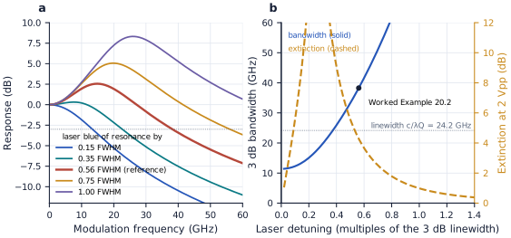
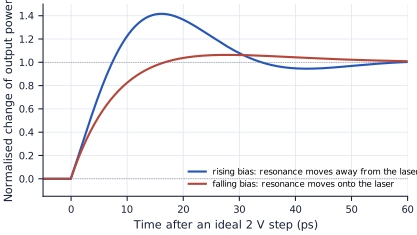
figsrc/ch20_rrm.py.A 2 Vpp swing moves the resonance by 100 pm, half a linewidth, so the small-signal picture is only a guide: across the swing the detuning varies from 0.30 to 0.82 linewidths, and the speed with it. Figure 20.2 shows the two edges for ideal voltage steps. When the reverse bias rises, the resonance moves away from the laser and the stored light escapes, beating with the laser: the output rises in 5.8 ps (10 to 90 %), overshooting by 42 %. When the bias falls, the resonance moves onto the laser and the ring must fill up: the output falls in 11.4 ps, with only 6 % overshoot. Rising and falling transitions therefore leave different intersymbol interference behind them, which a single linear equaliser cannot cancel at once.
figsrc/ch20_rrm.py.Carrier injection and pre-emphasis
Chapter 19 described the other silicon junction, a forward-biased PIN diode that floods the waveguide with electrons and holes. In a ring it is very efficient [81]. With the core weight of Chapter 19’s mode (0.92) and the Soref–Bennett relations, \(2.7\times10^{17}\) cm⁻³ of each carrier in the core of a 7.2 µm ring moves the resonance 291 pm blue, one and a half linewidths. Holding them there against recombination, with a 1 ns lifetime, takes 172 µA, about 155 µW at 0.9 V. The carriers also absorb: the intrinsic Q falls from 15 000 to 11 200.
Speed is the problem. The stored charge follows
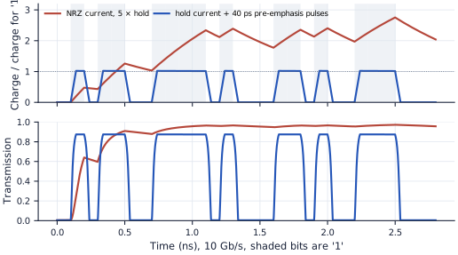
\[\frac{\mathrm{d}Q}{\mathrm{d}t} = I - \frac{Q}{\tau},\]so with the holding current alone the charge reaches only 9.5 % of its final value in a 100 ps bit at 10 Gb/s. Driving harder does not help (Figure 20.3, red): five times the holding current shifts the ring quickly at first, but the charge keeps piling up during runs of “1”s and drains with the 1 ns lifetime, so the “0”s after a run stay bright and the eye closes. Pre-emphasis shapes the current instead (blue). A short forward pulse at each rising edge delivers the charge of a “1” in 40 ps, the holding current keeps it, and a reverse pulse at each falling edge sweeps it out. The pulse needs 25 times the holding current, but because a diode’s current grows exponentially with its voltage, that takes only about 0.12 V more forward bias (ideality factor 1.5, series resistance neglected). The optical eye opens fully: the lowest “1” transmits 0.87, the highest “0” 0.004. The pulse width, the pulse depth and the DC bias all trade against each other, and a model that couples the diode’s charge to the ring’s optics is what lets a designer choose them.
figsrc/ch20_rrm.py.20.9Driving, linearising and locking a ring
High-swing drivers. A depletion ring with half the reference ring’s efficiency, 25 pm/V, needs 4 Vpp for the same 100 pm shift, four times the energy (80 fJ/bit at 20 fF), and more voltage than a thin-oxide CMOS transistor can switch [81]. Two techniques get there:
- Stacking. Output stages with cascoded transistors between two supply rails let each transistor see only part of the swing. Merging the main and post-cursor taps into one stack, rather than putting a stack in every segment, keeps any transistor from being overstressed during transitions and cuts the output capacitance.
- Differential, AC-coupled drive. Driving the cathode and the anode in antiphase doubles the swing across the junction, and coupling capacitors let each terminal sit at its own DC bias through a large resistor, so the junction stays reverse-biased whatever the supplies. With 2 pF coupling capacitors, 50 kΩ bias resistors and 70 fF of ring and pad capacitance, 97 % of the swing (−0.3 dB) reaches the ring, the high-pass corner is at 1.6 MHz, and a run of 72 identical bits at 50 Gb/s droops by only 1.4 %.
Because the two edges differ (Figure 20.2), ring drivers use an asymmetric FFE: the post-cursor tap is set separately for rising and falling transitions, or for the “1” and “0” levels.
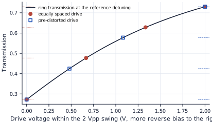
PAM4 on a ring. The Lorentzian bends the ring’s transfer curve. At the reference operating point, four equally spaced drive voltages give three eyes in the ratio 1.34 : 0.99 : 0.67 (Figure 20.4). The smallest eye sets the error rate, a penalty of 1.8 dB on top of PAM4’s 4.8 dB. Pre-distorting the drive, with levels at 0, 0.48, 1.08 and 2 V instead of 0, 0.67, 1.33 and 2 V, makes the eyes equal again. Transmitters do this with a DAC-based output stage and a look-up table that also applies a nonlinear FFE, or with a ring whose phase shifter is split into two segments, driven by the most and the least significant bit with independently set swings: an optical DAC [81, 82].
figsrc/ch20_rrm.py.Locking with data on. Locking a modulator differs from locking a drop filter (Chapter 18): data are on, and the target is not the resonance but a detuning. A common loop holds the average through-port power at a reference that a DAC sets, as a fraction of the input power [81]. At the reference point the average transmission is 0.50 and changes by 0.0046 per picometre of detuning, so even a 0.1 K drift (7.5 pm) moves it by 0.034: a strong error signal, and a monotonic one on the blue side of the resonance, where the loop runs. On the red side the slope reverses, so at start-up the controller heats the ring through the dip before it closes the loop. Two actuators can share the work:
- Heaters shift the ring red only, over a whole free spectral range, at about 0.26 nm/mW, but in tens of microseconds (Chapter 18).
- Bias is fast. A depletion ring’s DC bias moves it 50 pm per volt at almost no power, but ±1 V covers only ±0.67 K of drift, so bias suits fine, fast correction. An injection ring’s forward bias moves it blue far more efficiently than heat (0.28 nm for about 150 µW, against 1.1 mW for a heater), but its carriers add loss: the intrinsic Q falls from 15 000 to 11 300.
For a four-wavelength link the ring wins on size, energy (tens of femtojoules per bit against hundreds) and built-in multiplexing. The price is thermal control and a tight trade between Q, extinction and bandwidth. The MZM is broadband, needs no locking and has a large, clean eye, but it costs millimetres of chip, a few decibels more loss, a power-hungry driver, and a separate multiplexer. Short-reach WDM links with tight energy budgets choose rings; links that need robustness or coherent formats choose MZMs.
Four depletion ring modulators with U-shaped junctions (about 50 pm/V), \(Q_L \approx 8000\), driven with 2 Vpp NRZ by a CMOS driver with equalisation, each locked by its own heater loop. Expected: about 4 dB extinction at about 3 dB insertion loss, roughly 20 fJ/bit in the modulator.
Reading
- [36] Graham T. Reed, Goran Mashanovich, Frederic Y. Gardes and David J. Thomson. “Silicon optical modulators.” Nature Photonics, 4:518–526, 2010.
- [49] Cheng Wang et al. “Integrated lithium niobate electro-optic modulators operating at CMOS-compatible voltages.” Nature, 562:101–104, 2018.
- [32] Di Zhu et al. “Integrated photonics on thin-film lithium niobate.” Advances in Optics and Photonics, 13(2):242–352, 2021.
- [1] Lukas Chrostowski and Michael Hochberg. Silicon Photonics Design: From Devices to Systems. Cambridge University Press, 2015. https://www.cambridge.org/core/books/silicon-photonics-design/BF3CF13E8542BCE67FD2BBC7104ECEAB
- [74] Eduard Säckinger. Broadband Circuits for Optical Fiber Communication. Wiley-Interscience, 2005.
- [81] Sam Palermo. “Lecture 11: Ring Resonator Modulator Transmitters.” ECEN 721: Optical Interconnects Circuits and Systems, Texas A&M University, Spring 2026. https://people.engr.tamu.edu/spalermo/ecen689_oi/lecture11_ee721_rrm_tx.pdf
- Extinction ratio, OMA, insertion loss, bandwidth and energy per bit describe a modulator; OMA = 2Pavg(ER − 1)/(ER + 1).
- A 3 mm silicon MZM has Vπ ≈ 4.7 V: 2 Vpp gives about 6 dB of extinction at 6.3 dB of loss and about 0.4 pJ/bit in its termination.
- Travelling-wave electrodes need velocity and impedance matching; RF loss limits long silicon MZMs.
- Ring modulators use about 20 fJ/bit, but their Q trades extinction against bandwidth (c/λQ) and they need thermal locking.
- TFLN gives low-loss, linear, > 100 GHz modulators; EAMs are short but narrow-band; PAM4 halves the symbol rate for a 4.8 dB penalty.
- A detuned ring’s response peaks: the reference ring’s small-signal bandwidth rises from 12 GHz on resonance to 38 GHz at its operating point, at the cost of extinction. Its edges are unequal (5.8 and 11.4 ps), so drivers use asymmetric FFE.
- Carrier-injection rings are efficient but held back by the 1 ns carrier lifetime; pre-emphasis pulses of about 25 times the holding current open the eye.
- A ring bends PAM4 levels (a 1.8 dB penalty for the smallest eye) unless the drive is pre-distorted; ring modulators lock to an average-power reference with heaters, and fine-tune with bias.