Chapter 9Coupled-Mode Theory and Directional Couplers
Bring two waveguides close together and light moves back and forth between them; controlling that exchange is the basis of most passive devices.
- derive the coupled-mode equations for two waveguides, with and without phase mismatch;
- explain coupling with even and odd supermodes and the cross-over length;
- find the coupler length for any power split, and its dependence on gap, wavelength and polarisation;
- describe asymmetric, adiabatic and broadband couplers;
- write the 2 × 2 scattering matrix and explain its −j.
Which length and gap give a 50/50 split, and how robust is it?
9.1Coupled-mode equations
Two parallel waveguides a few hundred nanometres apart feel each other through their evanescent tails (Chapter 5). Write the total field as the two isolated modes with slowly varying amplitudes \(a_1(z)\) and \(a_2(z)\); the overlap of one guide’s field with the other’s index perturbation couples them [45]:
Here \(\kappa\) (per unit length) is the coupling coefficient. With all the light in guide 1 at \(z = 0\), the power in guide 2 is
\[P_2(z) = \frac{\kappa^2}{\kappa^2 + \delta^2}\sin^2\!\left(\sqrt{\kappa^2 + \delta^2}\,z\right), \qquad \delta = \frac{\beta_1 - \beta_2}{2}.\]For identical guides (\(\delta = 0\)) the power transfers completely and back again, with period \(\pi/\kappa\). For mismatched guides it transfers only partly, a fraction \(\kappa^2/(\kappa^2 + \delta^2)\), but faster. Phase matching is the condition for complete transfer: two waveguides of different widths barely couple, and a narrow and a wide guide can be designed to couple selectively between chosen modes (Chapter 8).
9.2Supermodes
There is a second, exact way to see the same physics. Two coupled identical waveguides form one structure whose own modes, the supermodes, are the even (symmetric) and odd (antisymmetric) combinations of the single-guide modes, with effective indices \(n_\mathrm{even} > n_\mathrm{odd}\). Light launched into one guide is half even and half odd; the two supermodes travel at different speeds, and after the length over which they slip by π relative to each other, they add up in the other guide. This cross-over length is
and a mode solver gives it directly: solve the pair of waveguides, read off the two indices, and subtract. This is the method used for the numbers below.
9.3The directional coupler
A directional coupler brings two waveguides together through S-bends, runs them in parallel for a length \(L\), and separates them again. The power crossing over is
\[\frac{P_\mathrm{cross}}{P_\mathrm{in}} = \sin^2\!\left(\frac{\pi(L + L_b)}{2L_x}\right),\]where \(L_b\) is the extra effective length contributed by the bends, which still couple while the guides are close. A 3 dB coupler needs \(L + L_b = L_x/2\).
Figure 9.1 shows \(L_x\) for two 500 × 220 nm silicon strips at 1550 nm (TE), computed with femwell. It grows exponentially with the gap, by about 2.4 times per 100 nm, because the coupling comes from tails that decay over about 100 nm.
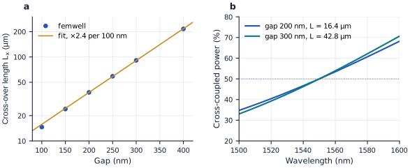
figsrc/part3_figs.py from figsrc/ch09_supermodes.py.At a 200 nm gap femwell gives \(n_\mathrm{even} = 2.4573\) and \(n_\mathrm{odd} = 2.4368\), so \(L_x = 1.55/(2 \times 0.0205) = 37.8\) µm. With the bends adding about 2.5 µm, a 50/50 coupler needs a straight section of \(37.8/2 - 2.5 = 16.4\) µm. At a 300 nm gap, \(L_x = 91\) µm and the straight section grows to 43 µm. A 100 nm gap would need only about 5 µm, but small gaps are hard to fabricate reproducibly, and a 10 nm error in a 100 nm gap changes \(L_x\) by about 10 %.
Try it. Set the gap, length and wavelength; the top view shows the light moving between the guides, and the cross-section the gap to scale.
9.4Wavelength, polarisation and fabrication sensitivity
A longer wavelength pushes more of each mode into the gap, so coupling grows quickly with wavelength: femwell gives \(L_x = 47\) µm at 1500 nm and 31 µm at 1600 nm for the 200 nm gap. A coupler designed for 50/50 at 1550 nm therefore splits 43.5/56.5 at 1530 nm and 57/43 at 1570 nm (Figure 9.1b), a drift of about 0.35 % per nanometre. TM modes, with longer tails, couple more strongly and have much shorter cross-over lengths. And because \(L_x\) is exponential in the gap and sensitive to width and thickness, fabrication variations move the split from die to die.
A directional coupler is the right choice when you need a specific, possibly small, coupling ratio at one wavelength: ring resonators (whose couplers are short directional couplers, Chapter 12), taps and monitors. It is the wrong choice for a broadband 3 dB split: across the 9.6 nm of the reference link’s channels the split above moves by about ±1.7 %, and across the C band by ±6 %.
9.5Broadband and adiabatic couplers
Three tricks flatten a coupler’s response:
- Asymmetric phase control. Using waveguides of slightly different widths in part of the coupler adds a wavelength-dependent phase that compensates the wavelength dependence of \(\kappa\). The broadband directional coupler of the SiEPIC EBeam PDK works this way [52]; see it in the 3D gallery.
- Adiabatic couplers. If one waveguide is tapered so that the input mode evolves slowly into the even or odd supermode of the symmetric section, the split ratio is set by symmetry, not by an interference length, and is nearly wavelength-independent, at the price of a device hundreds of micrometres long [53].
- Bent couplers. Curving the coupling region changes how the phase mismatch varies with wavelength and can cancel the dependence of \(\kappa\) over a band.
MMIs (Chapter 10) are the other broadband option.
9.6The 2 × 2 scattering matrix
Whatever happens inside, a lossless, reciprocal 2 × 2 coupler connects its input and output fields by a unitary, symmetric matrix. With power coupling \(\kappa^2\) (now meaning the coupled power fraction, not the coefficient per length) and \(t^2 = 1 - \kappa^2\):
\[\begin{pmatrix}b_1\\ b_2\end{pmatrix} = \begin{pmatrix} t & -j\kappa \\ -j\kappa & t\end{pmatrix}\begin{pmatrix}a_1\\ a_2\end{pmatrix}.\]The −j is not a convention to memorise but a consequence of energy conservation: unitarity requires the cross-coupled fields to be 90° out of phase with the through fields, so that \(\lvert b_1\rvert^2 + \lvert b_2\rvert^2 = \lvert a_1\rvert^2 + \lvert a_2\rvert^2\) for every input. That quadrature phase is what makes the Mach–Zehnder interferometer and the ring resonator of the next chapters work, and it is the same matrix used in their demos.
Free simulations by others that pair well with this chapter [11]:
Reading
- [45] Amnon Yariv. “Coupled-mode theory for guided-wave optics.” IEEE Journal of Quantum Electronics, 9(9):919–933, 1973.
- [1] Lukas Chrostowski and Michael Hochberg. Silicon Photonics Design: From Devices to Systems. Cambridge University Press, 2015. https://www.cambridge.org/core/books/silicon-photonics-design/BF3CF13E8542BCE67FD2BBC7104ECEAB
- [3] Katsunari Okamoto. Fundamentals of Optical Waveguides, 3rd edition. Academic Press, 2021.
- [52] Zeqin Lu, Han Yun, Yun Wang, Zhitian Chen, Fan Zhang, Nicolas A. F. Jaeger and Lukas Chrostowski. “Broadband silicon photonic directional coupler using asymmetric-waveguide based phase control.” Optics Express, 23(3):3795–3808, 2015. Open access.
- [53] Han Yun, Wei Shi, Yun Wang, Lukas Chrostowski and Nicolas A. F. Jaeger. “2×2 adiabatic 3-dB coupler on silicon-on-insulator rib waveguides.” Proc. SPIE 8915, Photonics North, 89150V, 2013.
- Coupled modes exchange power with period \(\pi/\kappa\); complete transfer needs phase matching.
- Equivalently, the even and odd supermodes beat: \(L_x = \lambda/(2\Delta n)\).
- For 500 × 220 nm silicon strips at 1550 nm: \(L_x = 37.8\) µm at 200 nm gap, growing 2.4× per 100 nm; a 3 dB coupler is about 16 µm long plus bends.
- A directional coupler’s split drifts by about 0.35 %/nm; use asymmetric, adiabatic or MMI couplers for broadband splitting.
- A lossless coupler’s matrix is unitary, and its −j cross-coupling phase is required by energy conservation.