Chapter 5The Slab Waveguide
A thin film of high index between two lower-index layers is the simplest waveguide, and most of what matters about guided light can be learned from it.
- explain guidance with the ray picture and the transverse-resonance condition;
- derive the TE and TM eigenvalue equations of an asymmetric slab;
- compute effective indices, field profiles, cut-offs and the number of modes;
- use the normalised V–b diagram;
- define the confinement factor and the evanescent decay length, and say why they matter for loss, coupling and sensing.
What sets the number of guided modes of a film, and their effective index?
5.1The ray picture and transverse resonance
Put a film of index \(n_1\) and thickness \(d\) between a substrate \(n_2\) and a cover \(n_3\), both lower. A ray inside the film that meets both interfaces beyond their critical angles is totally reflected at each (Chapter 2) and zig-zags along the film. Its wavevector \(n_1k_0\) splits into a component along the film, the propagation constant
\[\beta = n_1k_0\sin\theta = n_\mathrm{eff}\,k_0,\]which defines the effective index \(n_\mathrm{eff}\), and a transverse component \(\kappa = n_1k_0\cos\theta\) across it.
Not every angle survives. After one round trip across the film (down, reflect, up, reflect) the wave must add up in phase with itself, or successive reflections cancel. The round trip accumulates \(2\kappa d\) of phase from the path and loses \(2\phi_2 + 2\phi_3\) to the two reflections, whose phases come from the Fresnel coefficients beyond the critical angle. The transverse-resonance condition is therefore
Each integer \(m\) is a mode, a discrete angle, and therefore a discrete effective index. Guided modes have \(\max(n_2, n_3) < n_\mathrm{eff} < n_1\): below the lower bound the ray escapes into a cladding, and above the upper bound there is no real angle at all.
5.2TE and TM modes
The ray picture becomes exact when the reflection phases are written out. For a mode with \(\beta\), define the transverse wavenumber in the film and the decay constants in the claddings,
\[\kappa = k_0\sqrt{n_1^2 - n_\mathrm{eff}^2}, \qquad \gamma_2 = k_0\sqrt{n_\mathrm{eff}^2 - n_2^2}, \qquad \gamma_3 = k_0\sqrt{n_\mathrm{eff}^2 - n_3^2}.\]In TE modes the electric field lies in the plane of the film, perpendicular to the direction of propagation (\(E_y\) for a film in the \(y\)–\(z\) plane); \(E_y\) and its derivative must be continuous at both interfaces. In TM modes the magnetic field does that, and the continuity of \(H_y\) and of \((1/n^2)\,\partial H_y/\partial x\) brings in the index ratios. The field is a cosine in the film and an exponential tail in each cladding, and matching the four conditions gives the eigenvalue equation:
This is the transverse-resonance condition with \(\phi_i = \arctan(p_i/\kappa)\). Because \(n_1^2/n_i^2 > 1\), the TM reflection phases are larger, so a TM mode reaches resonance at a smaller \(\kappa\), which means a lower effective index: TM modes are less confined than TE modes in the same film.
The left-hand side falls and the right-hand side rises as \(n_\mathrm{eff}\) increases, so each \(m\) has at most one solution, found by bisection in a few lines of code. That is what the demo below does.
Try it. Change the thickness, wavelength and indices; the side view shows the film to scale with the zig-zag ray of each guided mode.
For silicon (\(n_1 = 3.476\)) in silica (\(n_2 = n_3 = 1.444\)), \(d = 220\) nm and \(\lambda_0 = 1550\) nm, solving the eigenvalue equation gives one TE mode with \(n_\mathrm{eff} = 2.848\) and one TM mode with \(n_\mathrm{eff} = 2.053\). The TE mode’s ray travels at \(\arcsin(2.848/3.476) = 55.0°\) from the normal; its transverse wavenumber is \(\kappa = 8.08\ \mu\mathrm{m}^{-1}\) and its field decays into the oxide with \(\gamma = 9.95\ \mu\mathrm{m}^{-1}\). With an air cover instead of oxide, the TE index drops only slightly, to 2.831, but the TM index falls to 1.891: TM modes feel the cladding far more.
5.3Effective index and normalised parameters
The slab problem depends on four numbers, but they combine into fewer. The normalised frequency (or V-number) and the normalised propagation constant are
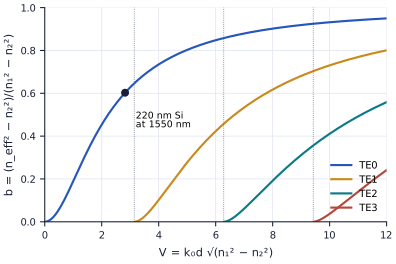
and \(b\) runs from 0 at cut-off (the mode is spread into the cladding) to 1 deep in the guiding regime (the mode sits almost entirely in the film). For a symmetric TE slab the eigenvalue equation becomes a universal relation between \(b\) and \(V\) alone,
\[V\sqrt{1 - b} = m\pi + 2\arctan\sqrt{\frac{b}{1 - b}},\]plotted in Figure 5.1. Any symmetric slab, of any material at any wavelength, is a point on these curves: thicker films, shorter wavelengths and higher contrast all move to the right.
figsrc/part2_figs.py.5.4Cut-off and the single-mode condition
A mode is cut off when \(n_\mathrm{eff}\) falls to the larger cladding index. In a symmetric slab (\(n_2 = n_3\)) that happens at \(V = m\pi\), so the fundamental TE0 and TM0 modes are always guided, however thin the film, and the slab is single-mode for
In an asymmetric slab (\(n_2 \neq n_3\)) even the fundamental mode has a cut-off, because the larger of the two reflection phases cannot always be matched: a very thin film on a substrate guides nothing.
For silicon in oxide at 1550 nm, \(\sqrt{n_1^2 - n_2^2} = 3.163\), so the slab is single-mode for \(d < 1.55/(2 \times 3.163) = 245\) nm. A 220 nm film is just below that limit: as thick as it can be while guiding only one TE and one TM mode vertically, which gives the strongest confinement without higher-order modes. A 300 nm film already guides TE1 (\(n_\mathrm{eff} = 1.685\)) and TM1 (\(n_\mathrm{eff} = 1.458\)). At 1310 nm the same 220 nm film is slightly multimode vertically in principle, but the second mode is weak and is cut off in narrow strips (Chapter 6). For silicon nitride in oxide (\(n_1 = 1.996\)) the limit is 562 nm, which is why SiN films are thicker.
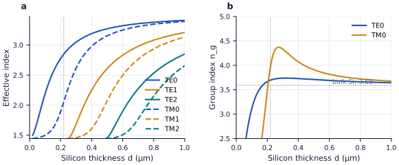
Figure 5.2 shows the effective index of the first modes against thickness for silicon in oxide. Every curve starts at the oxide index, where the mode appears, and approaches the silicon index as the film thickens.
figsrc/part2_figs.py.5.5Confinement and the evanescent field
Two numbers describe how much of a mode lives outside the film. The evanescent decay length \(1/\gamma\) is how far the field reaches into a cladding; the confinement factor \(\Gamma\) is the fraction of the mode’s power inside the film,
\[\Gamma = \frac{\int_\mathrm{film}\lvert E\rvert^2\,\mathrm{d}x}{\int_{-\infty}^{\infty}\lvert E\rvert^2\,\mathrm{d}x} \quad (\text{TE}).\]For the 220 nm silicon film at 1550 nm, \(1/\gamma = 101\) nm and \(\Gamma = 0.81\): one fifth of the power travels in the oxide. Both numbers set how a waveguide interacts with its surroundings. The evanescent tail is what a neighbouring waveguide couples to (Chapter 9), what a biosensor’s molecules perturb (Chapter 34), and what reaches through a too-thin buried oxide to leak into the silicon substrate (Chapter 7). The confinement factor reappears in lasers as the overlap of the mode with the gain (Chapter 24).
Strong confinement (large \(b\) and \(\Gamma\)) gives compact devices and tight bends, but it also concentrates the field at the interfaces, where sidewall roughness scatters light and where small thickness errors change the effective index most. Weak confinement does the opposite. Every platform choice in Chapter 4 is a position on this trade-off, and in silicon the 220 nm film sits close to the strongly confined end.
5.6Group index of a slab mode
The effective index of a mode changes with wavelength for two reasons: the materials are dispersive (Chapter 2), and the mode’s shape changes, because a longer wavelength pushes more of it into the low-index cladding. The second effect, waveguide dispersion, lowers \(n_\mathrm{eff}\) as \(\lambda\) grows, and so raises the group index \(n_g = n_\mathrm{eff} - \lambda\,\mathrm{d}n_\mathrm{eff}/\mathrm{d}\lambda\) above both the effective index and the bulk group index.
For the 220 nm film at 1550 nm the TE0 mode has \(n_\mathrm{eff} = 2.85\) but \(n_g = 3.70\), and the TM0 mode \(n_\mathrm{eff} = 2.05\) but \(n_g = 3.96\) (Figure 5.2b). Strong waveguide dispersion is a hallmark of high-contrast waveguides: in a silicon strip, where the light is confined in both directions, the group index reaches about 4.2 (Chapter 6).
Free simulations by others that pair well with this chapter:
Reading
- [3] Katsunari Okamoto. Fundamentals of Optical Waveguides, 3rd edition. Academic Press, 2021.
- [8] Allan W. Snyder and John D. Love. Optical Waveguide Theory. Chapman and Hall, 1983.
- [1] Lukas Chrostowski and Michael Hochberg. Silicon Photonics Design: From Devices to Systems. Cambridge University Press, 2015. https://www.cambridge.org/core/books/silicon-photonics-design/BF3CF13E8542BCE67FD2BBC7104ECEAB
- [2] Bahaa E. A. Saleh and Malvin C. Teich. Fundamentals of Photonics, 3rd edition. Wiley, 2019.
- A guided mode is a transverse resonance: \(2\kappa d - 2\phi_2 - 2\phi_3 = 2m\pi\), with \(n_\mathrm{eff} = n_1\sin\theta\) between the cladding and film indices.
- The slab eigenvalue equation \(\kappa d = m\pi + \arctan(p_2/\kappa) + \arctan(p_3/\kappa)\) covers TE and TM; TM modes are less confined.
- A symmetric slab is single-mode for \(V < \pi\); 220 nm of silicon in oxide is just below the 245 nm limit at 1550 nm.
- The 220 nm film’s TE0 mode has \(n_\mathrm{eff} = 2.85\), \(n_g = 3.70\), a 100 nm evanescent tail and 81 % of its power in the silicon.
- Waveguide dispersion pushes the group index well above the effective index in high-contrast guides.