Chapter 33Optical Links and Transceivers
Everything comes together in a link: laser, modulator, multiplexer, fibre, demultiplexer, detector, and the budget that connects them.
- describe IM-DD and coherent link architectures;
- compute a power budget with penalties and margin;
- turn extinction ratio, laser noise, threshold offset and intersymbol interference into power penalties;
- compare WDM transceiver architectures (parallel, CWDM, ring-based DWDM);
- estimate energy per bit including the laser’s wall-plug efficiency;
- check the reference link’s budget block by block;
- choose between NRZ and PAM4, and describe equalisers, clock recovery and a jitter budget;
- find which design choices cut the energy per bit.
Does the reference link close, and what does each block contribute?
33.1Link architectures
- Intensity modulation with direct detection (IM-DD) writes the data as optical power (NRZ or PAM4, Chapter 20) and detects it with a photodiode (Chapter 21). It is simple and low-power, and it rules short reaches: inside data centres, from metres to a few kilometres.
- Coherent links write the data onto the amplitude and phase of the field in both polarisations, and detect it by mixing with a local-oscillator laser, followed by digital signal processing that undoes dispersion and polarisation rotation. It carries more bits per symbol and reaches thousands of kilometres, at the cost of power-hungry DSP and narrow-linewidth lasers (Chapter 25).
Short-reach links scale capacity in three ways: faster lanes, more fibres (parallel single-mode, one fibre per lane) or more wavelengths per fibre (WDM).
An IM-DD transmitter puts the data on the light in one of two ways [76, 78]:
- Direct modulation drives the laser’s own current. It needs no extra component, but the carrier density, and with it the wavelength, swings with the current, so the light is chirped (Chapter 25). The laser must also stay above threshold for a “0”, or every “1” starts late by a delay that depends on the pattern, which caps the extinction ratio. The VCSEL, a laser that emits from its surface, is the cheapest transmitter of all; its bandwidth grows with the square root of the bias above threshold, so speed costs current and extinction [79]. VCSELs at 850 nm over multimode fibre serve the shortest links, inside racks and rows; directly modulated DFB lasers serve single-mode links near 1310 nm, where the fibre’s dispersion is small.
- External modulation keeps a continuous-wave laser on and modulates its light (Chapter 20): with a Mach–Zehnder modulator (broadband and robust, but millimetres long and driven with several volts [80]), an electro-absorption modulator (short, a small capacitance), or a ring (micrometres and femtojoules, wavelength-selective, but in need of a lock). Without chirp, the spectrum is as narrow as the data allow, which is what lets the reference link run over 2 km at 1550 nm.
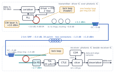
At the far end, a photodiode feeds a transimpedance amplifier (TIA), usually followed by an equaliser and a gain stage, then a decision circuit (the slicer) clocked by a clock-and-data-recovery circuit (CDR), and a deserialiser [77, 87]. Figure 33.1 draws one lane of the reference link this way, with the power at each point of the optical path; Chapter 1 shows all four lanes.
figsrc/ch33_links.py.33.2Power budget and penalties
The budget of Chapter 1 subtracts each block’s loss from the launched power and compares the received power with the receiver’s sensitivity. A real budget also subtracts penalties: the extra power needed because the signal is not ideal.
- Extinction ratio: a finite ER wastes average power on the “0” level (Chapter 21 already includes the 4 dB ER in its −11.6 dBm sensitivity).
- Crosstalk: light from neighbouring channels leaking through the demultiplexer adds noise and a power penalty. With −20 dB of adjacent-channel rejection (Chapter 14) the two neighbours leak about 2 % of the power, a penalty of roughly 0.1 dB; the budget allows a generous 0.5 dB.
- Dispersion and chirp: 2 km at 1550 nm accumulate 34 ps/nm (Example 2.5), inside the 40–60 ps/nm tolerance of 50 Gb/s NRZ but not free: a few tenths of a decibel with a chirp-free modulator, more with chirp, so the budget allows 0.5 dB. Directly modulated lasers, with their large chirp, fare much worse (Chapter 25).
- Noise and jitter: laser RIN, electrical jitter and intersymbol interference from limited bandwidth.
- Drift and ageing: rings slightly off their lasers, lasers that lose power over their lifetime.
A link closes when the margin is positive; designers keep a few decibels in reserve for what was not modelled.
BER, Q and sensitivity
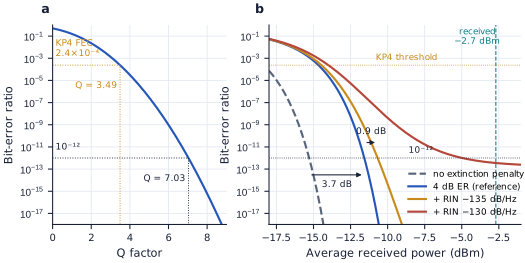
Chapter 21 related the bit-error ratio to the Q factor, the gap between the “0” and “1” levels in units of the noise. Figure 33.2a plots the relation: a BER of 10⁻¹² needs Q = 7.03, 10⁻¹⁵ needs 7.94, and the KP4 FEC threshold only 3.49. The sensitivity is the average power at which a receiver reaches a target BER, so a sensitivity means nothing without its BER [77]. Because the BER falls as the tail of a Gaussian, its curve against received power is steep (Figure 33.2b): the reference receiver reaches 10⁻¹² at −11.6 dBm, 1.8 × 10⁻¹⁵ half a decibel higher, and 7 × 10⁻¹⁹ one decibel higher. That is why budgets are kept in decibels of power at a fixed BER, not in error ratios.
Standards often quote the receiver’s OMA sensitivity instead [78]. It leaves the extinction ratio out of the receiver’s number and puts it on the transmitter’s account; for the reference receiver it is about 60 µW, or −12.2 dBm, with shot noise included.
Penalties in decibels
A power penalty is the extra average power an impairment costs at a fixed BER, quoted in decibels [77, 78, 79]. In a receiver limited by its TIA’s noise, four of them have simple forms:
each in decibels as \(10\log_{10}\mathrm{PP}\). Here \(r\) is the extinction ratio (the penalty is against a perfect one); RIN is the laser’s relative intensity noise per hertz, as a plain number, and \(B_n\) the noise bandwidth (this form holds for a high extinction ratio); \(\Delta\) is the offset of the decision threshold from its best value and \(\sigma\) the rms noise; and \(h_k\) are samples of the received pulse one bit apart, with \(h_0\) the main one, so that the last form is the worst case over all data patterns (peak distortion). Timing errors are the fifth penalty; Section 33.10 gives them a budget of their own.
Take the receiver of Worked Example 21.2 (0.9 A/W, 20 pA/√Hz over a 35 GHz noise bandwidth, so σ = 3.7 µA), which reaches 10⁻¹² at −11.6 dBm with the ring’s 4 dB extinction.
- Extinction. \(r = 2.5\) gives PP = 3.5/1.5 = 2.33, or 3.7 dB, already inside the −11.6 dBm. A 6 dB modulator would cost 2.2 dB and a 10 dB one 0.9 dB: the ring’s modest extinction is the largest single penalty in the link, which is why Chapter 20 fought for every decibel of it.
- Laser noise. At RIN = −140 dB/Hz, the requirement of Chapter 25, the penalty is 0.26 dB. With a high extinction ratio it would be only 0.08 dB: at 4 dB the “0” level still carries 40 % of the power of the “1”, and its noise with it. At −135 dB/Hz the penalty grows to 0.9 dB, and at −130 dB/Hz to 6.6 dB, with a floor at 1.7 × 10⁻¹³ that no power can beat, because signal and noise then grow together (Figure 33.2b).
- Offset. A decision threshold half a noise rms (1.9 µA) from its best value costs 0.24 dB; the receiver’s offset-cancellation loop must keep it smaller.
- Bandwidth. A transmitter modelled as a single pole at 24 GHz, the optical bandwidth of the reference ring (Chapter 20), and a receiver with a second-order Butterworth response at 32 GHz close the 50 Gb/s eye by 1.1 dB in the worst case. The driver’s equalisation and the ring’s detuning peaking must win that back (Section 33.9).
Apart from the extinction penalty, which the sensitivity already contains, none of these is among Table 33.1’s allowances. With the RIN at −140 dB/Hz and the offset trimmed to half a noise rms they add 0.5 dB, which the 5.9 dB margin absorbs; the bandwidth penalty has to be equalised away.
figsrc/ch33_links.py.33.3WDM transceivers
- Parallel single-mode transceivers use one fibre per lane (four transmit and four receive), with identical lasers and modulators. Simple optics, but many fibres.
- CWDM transceivers multiplex four lanes 20 nm apart near 1310 nm onto one fibre, with uncooled lasers and broadband filters (MZI lattices or echelle gratings, Chapter 14).
- Ring-based DWDM, the reference link’s architecture, uses ring modulators that also multiplex, and drop rings that demultiplex, on a dense grid. It is compact and energy-efficient and scales to many wavelengths, with every ring locked to its laser (Chapter 18).
Locking one ring is a feedback loop (Chapter 18); locking a ring-based transceiver is a system task [87]. At start-up, each heater sweeps its ring across the lasers and the controller decides which ring takes which channel. The 7.2 µm rings have a free spectral range of 13.7 nm, which holds 4.3 channels of the 400 GHz (3.2 nm) grid, so letting each ring take the nearest laser, with the data reordered electronically, limits the heater power that fabrication errors cost. In operation the loops must ignore each other’s heat, follow the self-heating that the data pattern causes in a modulator ring, and hold each modulator not on its resonance but at the detuning that gives the best OMA, for example by holding its average output power at a set fraction of its input (Section 20.9). A lost lock is a dead lane, so the loops’ speed and their recovery belong to the link’s reliability budget.
33.4Coherent transceivers
A coherent transmitter uses an IQ modulator, two nested Mach–Zehnder modulators biased at null with a 90° phase shift between them, in each polarisation, combined by a polarisation rotator and combiner (Chapter 14). The receiver mixes the signal with a local oscillator in a 90° optical hybrid (an MMI, Chapter 10) feeding balanced photodiodes, and the DSP recovers the symbols. Silicon photonics integrates the modulators, hybrids and detectors; thin-film lithium niobate offers lower-loss, more linear modulators (Chapter 20).
33.5Energy per bit
The figure of merit of a short-reach link is its total energy per transmitted bit. For a WDM link it adds up as
\[E_\mathrm{bit} = \frac{N_\lambda P_\mathrm{opt}/\eta_\mathrm{wp} + P_\mathrm{heaters} + P_\mathrm{drivers} + P_\mathrm{RX}}{\text{total bit rate}}\]The laser term is usually the largest, because the optical power in the waveguide is divided by a wall-plug efficiency \(\eta_\mathrm{wp}\) of 10–20 % once coupling losses and the laser’s own efficiency (Chapter 24) are counted. Every decibel of loss saved in the link can be turned into laser power saved. Heaters come next for ring-based designs (Chapter 18). Modulators themselves are almost free: 20 fJ/bit for a ring (Chapter 20).
33.6Co-packaged optics
As switch and accelerator chips pass tens of terabits per second, driving signals across a circuit board to pluggable modules costs too much power. Co-packaged optics places the photonic chips on the same package as the switch, with millimetre-long electrical connections (Chapter 17). The lasers often stay outside, in replaceable modules, feeding the package through fibre. Ring-based WDM, with its small size and low energy per bit, is a natural fit, which is why the reference link is built that way.
Between today’s pluggables and co-packaged optics sits linear-drive optics. A conventional pluggable module retimes the signal: a DSP chip recovers the clock and equalises in each direction, and spends a large share of the module’s power doing so. A linear-drive module leaves the DSP out and passes the host’s signal through linear drivers and TIAs, so the host’s own equaliser must treat the optics as part of its channel. It saves the retimer’s power, but asks for very linear, broadband analogue electronics [76, 87].
33.7The reference link, block by block
Table 33.1 closes the budget set in Chapter 1 with the numbers each chapter produced; where no chapter computed a value, Chapter 1’s estimate or an allowance stands.
Table 33.1. The reference link: 4 × 50 Gb/s NRZ over 2 km, one wavelength.
| Block | Value | Chapter |
|---|---|---|
| Laser power in the transmitter waveguide | +10 dBm | 1 (target), 24–27 |
| Ring modulator insertion loss | −3.0 dB (4 dB ER at 2 Vpp, about 50 pm/V) | 19, 20 |
| Other rings and routing | −0.8 dB | 1 (estimate) |
| Transmit grating coupler | −3.0 dB (−4 dB for the measured PDK design) | 15 |
| 2 km of fibre and two connectors | −0.4 dB, −1.0 dB | 3; 1 (connectors, estimate) |
| Receive grating coupler | −3.0 dB | 15 |
| Demultiplexing ring and routing | −1.5 dB | 1 (estimate), 14 |
| Received power | −2.7 dBm | 1 |
| Receiver sensitivity at BER 10⁻¹² (4 dB ER) | −11.6 dBm | 21 |
| Penalties: crosstalk, dispersion, drift and locking, ageing | 0.5 + 0.5 + 1.0 + 1.0 dB | allowances (2, 14, 18) |
| Margin | 5.9 dB | |
| Energy: lasers (15 % wall plug), heaters, TIAs, drivers, modulators | 1.33 + 0.80 + 1.0 + 0.5 + 0.02 = 3.65 pJ/bit | 18, 20; TIAs and drivers: typical values |
The link closes with 5.9 dB of margin and uses about 3.7 pJ/bit against the 5 pJ/bit target. The weakest points are the ones the earlier chapters flagged: the ring modulator’s tight trade between extinction, loss and bandwidth (Chapter 20), the grating couplers (with the measured PDK design at −4 dB each, the margin drops to 3.9 dB), and the heater power, which depends on the fabrication spread (Chapter 29). The margin could also be spent on cutting the laser power: 2.9 dB less light per lane saves 0.65 pJ/bit and still leaves the 3 dB the targets ask for.
Try it. Change any block, the laser’s wall-plug efficiency or the heater power, and watch the budget and the energy per bit.
33.8NRZ or PAM4
The power budget is one of three that a link must close. The other two are the shape of the signal, its format and the equalisation that keeps it clean, and its timing. This section and the next two check them for the reference link.
Chapter 20 gave PAM4’s price at equal swing: three eyes, each a third as tall as the NRZ eye, or 4.8 dB of optical power. At equal bit rate, PAM4 also halves the symbol rate, which halves the noise bandwidth and gives back 1.5 dB, so the net cost in a thermal-noise-limited receiver is 3.3 dB. With shot noise and PAM4’s extra error events included, the reference receiver needs −6.6 dBm for 100 Gb/s PAM4 at 10⁻¹², against −10.0 dBm for 100 Gb/s NRZ: 3.4 dB more.
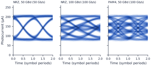
What PAM4 buys is bandwidth. A rule from electrical links carries over: PAM4 beats NRZ when the channel loses more than \(20\log_{10}3 = 9.5\) dB over the octave between the two formats’ Nyquist frequencies, half the PAM4 symbol rate and half the NRZ one [83]. In a short optical link the “channel” is mostly the transceiver’s own parts. With the transmitter modelled as a single pole at the ring’s 24 GHz optical bandwidth, and a receiver with a second-order Butterworth response at 32 GHz (whose noise bandwidth, 35 GHz, is Chapter 21’s), the front end loses 4.6 dB at 25 GHz and 15.7 dB at 50 GHz: 11.1 dB over the octave. Figure 33.3 shows the result. In the worst case, intersymbol interference closes a 100 GBd NRZ eye by 9.5 dB, but the 50 GBd PAM4 eyes by only 2.6 dB, on top of their 4.8 dB.
figsrc/ch33_links.py.PAM4 has costs beyond the decibels [83, 82]. The receiver needs three slicers whose thresholds must follow the levels. Transitions between non-adjacent levels cross the thresholds at different times, which adds jitter for the CDR. The smaller eyes suffer more from crosstalk and residual ISI. And the modulator must be linear, or the levels pre-distorted: a ring’s Lorentzian response squeezes the outer levels. One answer splits the ring’s phase shifter into two segments, one twice as long as the other, driven by the most and the least significant bit, so that the ring itself adds two NRZ streams into four levels, an optical DAC. In practice, PAM4 links run with forward error correction.
There are three ways to double the reference link to 400 Gb/s.
- Eight wavelengths at 50 Gb/s NRZ. The 7.2 µm rings’ 13.7 nm free spectral range holds only 4.3 channels at 3.2 nm, so eight channels need the 200 GHz grid, with tighter crosstalk (Chapter 14), or smaller rings; and four more lasers, drivers, receivers and heater loops.
- Four lanes at 100 GBd NRZ. Besides the 9.5 dB of ISI above, the dispersion tolerance falls as the square of the symbol rate: from 40–60 ps/nm at 50 GBd (Example 2.5) to 10–15 ps/nm at 100 GBd, against the 34 ps/nm of 2 km at 1550 nm. NRZ at 1550 nm runs out of tolerance between about 54 and 66 GBd.
- Four lanes at 50 GBd PAM4. The optics and the symbol rate stay as they are, and the dispersion tolerance stays close to NRZ’s (somewhat lower, as the eyes are smaller). The receiver needs −6.6 dBm at 10⁻¹², which leaves 0.9 dB of margin after the 3.0 dB of allowances, short of the 3 dB target. At the KP4 threshold it needs −9.9 dBm, which leaves 4.2 dB, from which PAM4’s larger ISI and dispersion penalties must still be paid.
PAM4 with FEC is the only one of the three that keeps the reference link’s optics, which is why links at 100 Gb/s per wavelength and beyond use PAM4.
33.9Drivers and equalisation
The driver has to give the modulator the swing it needs at the speed it needs (Chapter 20):
- A laser’s light follows its current above threshold, so laser and VCSEL drivers are current-mode: a bias current keeps the laser above threshold, and a switched modulation current carries the data [79].
- A ring or an EAM is a small capacitor, so a CMOS voltage-mode driver, essentially an inverter, can drive it. When the modulator needs more swing than one transistor can stand, stacked (cascoded) output stages switch between two supply rails, so that each transistor sees only part of the voltage [76, 82].
- A travelling-wave MZM is a terminated transmission line that takes several volts into tens of ohms; a segmented MZM splits it into short sections driven by CMOS inverters [80].
Equalisation undoes the intersymbol interference of the channel, and in a short optical link the channel is mostly the transceiver itself: driver, modulator, photodiode and TIA. Three equalisers are used, alone or together [84, 77]:
- A feed-forward equaliser (FFE) in the transmitter, an FIR filter that subtracts scaled copies of the neighbouring bits from each bit. It adds no noise, but the driver’s peak swing is fixed, so the FFE boosts the high frequencies by giving up low-frequency amplitude (de-emphasis).
- A continuous-time linear equaliser (CTLE) in the receiver, an amplifier whose gain peaks near the Nyquist frequency. It is cheap and fast, but amplifies the noise along with the signal.
- A decision-feedback equaliser (DFE), which subtracts the ISI of bits already decided. It adds no noise, but cannot remove the ISI from bits still to come (the pre-cursor), and its feedback must settle within one bit.
The taps are usually adapted in operation, for example by a sign–sign LMS loop that nudges each tap according to the signs of the error and of the data.
Rings add two twists. A ring responds differently to rising and falling edges: the light stored in it escapes faster when the resonance moves away from the laser than it builds up when the resonance moves onto it (5.8 against 11.4 ps for the reference ring, Section 20.8). So ring drivers use asymmetric FFE, with separate taps for the two edges [81, 82]. And the receiver’s bandwidth trades noise against ISI: the narrower it is, the less noise it collects but the more ISI it adds [77]. For a second-order Butterworth front end at 50 Gb/s the ISI penalty is 1.4 dB at a 3 dB bandwidth of 0.4 B, 0.25 dB at 0.5 B and negligible above 0.55 B, while the noise grows as the square root of the bandwidth; the sum is within 0.3 dB of its minimum from 0.45 B to 0.63 B. Chapter 21’s noise bandwidth of 0.7 B corresponds to 0.63 B for this response, at the wide end of that range. Some receivers go further: a TIA with a bandwidth well below the optimum can use a larger feedback resistor, with less noise, and a CTLE after it restores the bandwidth [82].
Suppose a transmitter’s response at 50 Gb/s is a single pole at 12.5 GHz, a quarter of the bit rate: a VCSEL at low bias, say, or a ring with a higher Q. Each bit then leaks 0.21 of its main sample into the next bit, and less into later ones. In the worst case the eye is 0.58 of the full swing, and the zero crossings wander by 3.0 ps peak to peak with the data pattern.
A two-tap FFE with taps 0.83 and −0.17 (their magnitudes sum to one, the driver’s full swing) cancels every post-cursor of a single pole exactly. The eye grows to 0.66 of the swing and the pattern-dependent jitter vanishes. The vertical gain is only 0.5 dB, because the main tap gave up swing to pay for the second: long runs of identical bits now reach only 66 % of the full swing. The larger gain is in time, where the 3.0 ps of jitter was 15 % of the bit.
33.10Clocking, jitter and the timing budget
Every bit must be sampled near its centre, and the reference link sends no clock alongside its data: the receiver recovers it from the data’s transitions [86]. A CDR is a phase-locked loop whose phase detector works on random data. The most common, the bang-bang (Alexander) detector, samples each bit at its centre and at its edge; when two successive bits differ, the edge sample shows whether the clock is early or late. A loop filter integrates these votes and moves the clock phase, through the oscillator of a single-loop CDR or through a phase interpolator that mixes phases of a shared PLL’s clock (a dual-loop CDR). Without transitions there is no information, which is why links scramble or encode their data.
A CDR follows jitter slower than its loop bandwidth and passes it on (its jitter transfer). Faster jitter it cannot follow, so the eye must absorb it: at high frequencies a receiver’s jitter tolerance is its eye opening at the target BER. In a WDM link each lane needs its own phase, because the lanes arrive at different times: across the reference link’s 9.6 nm, the fibre’s 34 ps/nm delays them by up to 327 ps, more than 16 bits. The lanes can share the transmitter’s PLL and a receiver PLL, with a phase interpolator or a CDR per lane.
Jitter comes in two kinds [85]. Random jitter (RJ), from device noise, is Gaussian and unbounded, and is quoted as an rms value. Deterministic jitter (DJ) is bounded: duty-cycle distortion from the serialiser’s clocks, ISI (pattern-dependent crossings, as in Worked Example 33.3), periodic jitter from supplies and reference clocks, and jitter induced by crosstalk from other lanes. The dual-Dirac model replaces the deterministic part by two delta functions DJ apart, and gives the total jitter at a BER:
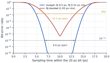
Deterministic terms add linearly and random ones in quadrature, with \(2Q_\mathrm{BER}\) = 14.07 at 10⁻¹² but only 6.98 at the KP4 threshold [77, 85]. Table 33.2 is an illustrative budget for the reference link’s 20 ps bit, and Figure 33.4 its bathtub curve, the BER against the sampling instant.
Table 33.2. An illustrative jitter budget for the reference link (50 Gb/s NRZ, UI = 20 ps).
| Source | DJ (ps, peak to peak) | RJ (ps rms) |
|---|---|---|
| Transmitter: serialiser, driver, ring | 2.0 | 0.30 |
| Modulator and fibre ISI, after FFE | 2.0 | – |
| Receiver front end: TIA, CTLE | 1.0 | 0.25 |
| Clock: PLL and CDR | 1.0 | 0.35 |
| Total | 6.0 | 0.52 |
| TJ at 10⁻¹² (DJ + 14.07 RJ) | 13.4 ps: 6.6 ps (0.33 UI) open | |
| TJ at the KP4 threshold (DJ + 6.98 RJ) | 9.7 ps: 10.3 ps (0.52 UI) open |
The eye stays open by 6.6 ps at 10⁻¹², a third of the bit, and that is also the fast jitter the receiver can tolerate. Random jitter is the sensitive term, because it is multiplied by 14: doubled to 1.05 ps rms, it closes the eye at 10⁻¹² (a total of 20.8 ps), and anything above 1.0 ps rms does so. At the KP4 threshold the doubled jitter still leaves 6.7 ps open. FEC buys timing margin as well as power margin.
figsrc/ch33_links.py.33.11Optimising for energy
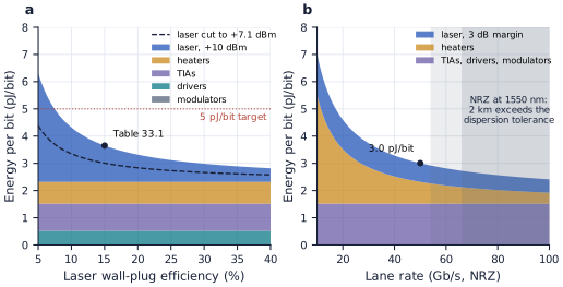
Table 33.1 spends 3.65 pJ/bit. Figure 33.5 asks what moves it.
- Wall-plug efficiency. The laser term is optical power divided by efficiency, so it dominates when the efficiency is poor (Figure 33.5a). At +10 dBm per lane the link meets 5 pJ/bit down to 7.5 % wall-plug efficiency; at 30 % it would use 3.0 pJ/bit, the same as spending 2.9 dB of margin on less light at 15 % (Section 33.7).
- Margin. Margin is laser power held in reserve. Lasers sized for exactly 3 dB of margin, +7.1 dBm per lane, bring the link to 3.0 pJ/bit.
- Lane rate. Heater power is fixed per ring whatever the data rate, while the laser power needed rises only as the square root of the rate, since the receiver’s noise grows with its bandwidth. So the energy per bit falls as lanes get faster (Figure 33.5b): 4.1 pJ/bit at 25 Gb/s, 3.0 at 50 and 2.4 at 100 Gb/s, with the electronics held at Table 33.1’s 1.5 pJ/bit. Two things end the trend: dispersion, which stops NRZ at 1550 nm over 2 km between 54 and 66 Gb/s (Section 33.8), and the electronics, whose energy per bit rises as they near their technology’s speed limit.
- Trading blocks. Every decibel of sensitivity saves a decibel of laser power. A TIA with half the noise current (10 pA/√Hz) improves the sensitivity by 2.9 dB, which is worth 0.34 pJ/bit of laser energy at the 3 dB-margin operating point; it pays if it costs less than 17 mW more per lane. FEC buys 3.1 dB in the same way (Chapter 21), at the price of its encoder, decoder and latency. Undercut heaters, at 0.15 instead of 0.8 pJ/bit (Chapter 18), are the other large saving.
- Electronics architecture. A receiver spends most of its energy in its analogue front end [82]. A CTLE costs less than a DFE where the ISI allows it, and clocks generated on chip and shared among lanes save the power of distributing them.
figsrc/ch33_links.py.Reading
- [28] Sudip Shekhar, Wim Bogaerts, Lukas Chrostowski, John E. Bowers, Michael Hochberg, Richard Soref and Bhavin J. Shastri. “Roadmapping the next generation of silicon photonics.” Nature Communications, 15:751, 2024. Open access.
- [1] Lukas Chrostowski and Michael Hochberg. Silicon Photonics Design: From Devices to Systems. Cambridge University Press, 2015. https://www.cambridge.org/core/books/silicon-photonics-design/BF3CF13E8542BCE67FD2BBC7104ECEAB
- [55] Chen Sun et al. “Single-chip microprocessor that communicates directly using light.” Nature, 528:534–538, 2015.
- [74] Eduard Säckinger. Broadband Circuits for Optical Fiber Communication. Wiley-Interscience, 2005.
- [75] Sam Palermo. ECEN 721: Optical Interconnects Circuits and Systems, course page and lecture slides, Texas A&M University, Spring 2026. https://people.engr.tamu.edu/spalermo/ecen721.html
- IM-DD rules short reaches; coherent links carry more per symbol over long distances with DSP.
- Margin = launch power − losses − penalties − sensitivity; keep a few decibels in reserve.
- Penalties are decibels of extra power at a fixed BER: the ring’s 4 dB extinction costs 3.7 dB, RIN must stay near −140 dB/Hz or below (0.26 dB), and −130 dB/Hz would put a floor under the BER.
- Parallel, CWDM and ring-based DWDM trade fibres, filters and control.
- Energy per bit is dominated by laser wall-plug power and, for rings, heaters; modulators are nearly free.
- The reference link closes with 5.9 dB of margin at about 3.7 pJ/bit; its tight spots are the ring modulator, the couplers and the heaters.
- PAM4 costs about 3.4 dB against NRZ at equal bit rate but halves the symbol rate; it wins when the channel loses more than 9.5 dB over the octave below the NRZ Nyquist frequency, so 400 Gb/s on the reference link’s four wavelengths needs PAM4 and FEC.
- FFE, CTLE and DFE win back bandwidth, a CDR recovers the clock, and the timing budget DJ + 2Q·RJ must fit in the bit: 6.6 ps of 20 ps stay open at 10⁻¹² in the illustrative budget.
- Energy per bit falls with better wall-plug efficiency, with less spare margin and with faster lanes, until dispersion or the electronics stop it.