Chapter 4Materials and Platforms: Si, SiN, TFLN, BTO and InP
Silicon is the workhorse, but no single material does everything: the platform is chosen by what the chip must do.
- list what a photonic platform must provide: guiding, tuning, modulating, detecting, generating and amplifying light;
- compare Si, SiN, thin-film LiNbO₃, BaTiO₃ and InP by index, transparency, loss, electro-optic and thermo-optic response, and gain;
- describe the layer stack and typical waveguide of each platform;
- distinguish monolithic, hybrid and heterogeneous integration;
- find the foundry and MPW routes and the open PDKs that this tutorial uses.
Which platform for which job, and when is one platform not enough?
4.1What a platform must provide
A photonic platform is a material system plus a manufacturing process plus a design kit. A complete transceiver needs six functions from it: guide light with low loss and tight bends, tune it slowly (for calibration and locking), modulate it fast, detect it, generate it and amplify it. Table 4.1 shows which platforms provide which functions natively; the gaps are why most real products combine materials.
Table 4.1. Native capabilities of the main platforms. ● native, ◐ only with an added material or a bonded or attached chip, ○ not available.
| Function | Si (SOI) | SiN | TFLN | BTO on Si | InP |
|---|---|---|---|---|---|
| Low-loss guiding, tight bends | ● tight bends, moderate loss | ● lowest loss, larger bends | ● | ● | ● larger bends |
| Thermal tuning | ● efficient | ● weaker | ● | ● | ● |
| Fast modulation | ● carrier depletion | ○ | ● Pockels | ● Pockels | ● electro-absorption, QCSE |
| Detection at 1310/1550 nm | ● germanium | ◐ | ◐ | ◐ via Si/Ge | ● InGaAs |
| Light generation and gain | ◐ III–V attached or bonded | ◐ | ◐ | ◐ | ● |
| CMOS-foundry manufacturing | ● | ● | ○ | ◐ | ○ |
4.2The materials
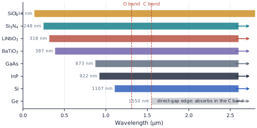
Table 4.2 collects the material properties behind Table 4.1, and Figure 4.1 shows where each material is transparent. The short-wavelength edge of transparency is set by the bandgap: a photon with more energy than the gap is absorbed, so the edge is at \(\lambda_g = hc/E_g = 1.24/E_g[\mathrm{eV}]\) µm.
Table 4.2. Photonic materials at 1550 nm. Approximate room-temperature values; deposited and thin-film materials vary with process.
| Material | Index | Bandgap | Thermo-optic dn/dT | Electro-optic effect |
|---|---|---|---|---|
| Silicon | 3.48 | 1.12 eV, indirect | ≈ 1.8 × 10⁻⁴ /K | free-carrier plasma dispersion only [40] |
| Silica | 1.44 | ≈ 9 eV | ≈ 1 × 10⁻⁵ /K | none |
| Silicon nitride | ≈ 2.0 | ≈ 5 eV | ≈ 2.5 × 10⁻⁵ /K | none (stress-optic and thermal tuning) |
| Lithium niobate | 2.21 (o), 2.14 (e) | ≈ 4 eV | — | Pockels, r₃₃ ≈ 30 pm/V [32] |
| Barium titanate | ≈ 2.3 | ≈ 3.2 eV | — | Pockels, hundreds of pm/V in thin films [33] |
| Indium phosphide | 3.17 | 1.34 eV, direct | — | weak Pockels; electro-absorption in quantum wells |
| Germanium | ≈ 4.3 | 0.66 eV indirect, 0.80 eV direct | — | Franz–Keldysh electro-absorption |
figsrc/part1_figs.py.Three properties decide most platform choices:
- Index contrast sets how tightly light is confined, and therefore how small waveguides and bends can be. Silicon against silica (\(\Delta n \approx 2\)) is at one extreme; InGaAsP against InP (\(\Delta n \approx 0.2\) in the vertical direction) at the other, which is why InP waveguides are etched deeply to confine light sideways.
- The electro-optic effect decides how fast and efficiently a phase can be changed. Only non-centrosymmetric crystals (LiNbO₃, BaTiO₃, the III–Vs) have a Pockels effect, a change of index proportional to the applied field. Silicon must instead move free carriers, which changes both index and absorption.
- The bandgap decides absorption and gain. Light can only be generated efficiently in a direct-gap semiconductor, and detected in one whose gap is below the photon energy.
4.3Silicon-on-insulator
The standard silicon-photonics wafer is SOI: a crystalline silicon film on a buried oxide on a silicon handle wafer. The film is most often 220 nm thick, a value that grew out of early CMOS-compatible processes and is now the default of most foundry PDKs; 300–340 nm films are used for lower loss and easier coupling, and 3 µm films (VTT) for very low loss and polarisation-independent operation [20]. The BOX is 2–3 µm thick, enough to keep the guided mode from leaking into the silicon handle at 1550 nm (thinner BOX is a problem at longer wavelengths, Chapter 7).
A full silicon-photonics process adds partial etches for rib waveguides and grating couplers, implants for p–n junction modulators, germanium epitaxy for detectors, metal heaters and two or more metal layers, and sometimes a silicon nitride layer above the silicon. Its strengths are density (bends of a few micrometres), fast and mature modulators and detectors, and the volume and statistics of CMOS fabs. Its weaknesses are the ones listed in Chapter 1: no laser, propagation losses of 1–3 dB/cm in strip waveguides, two-photon absorption, and high sensitivity to temperature and to nanometre variations.
Silicon photonics is available through many foundries and MPW services, among them AMF, AIM Photonics, imec, GlobalFoundries, Tower Semiconductor, CORNERSTONE, VTT, and Applied Nanotools with SiEPICfab for electron-beam prototyping [29, 14]. Their PDKs differ in film thickness, layers and rules; the open ones are listed in Section 4.8.
4.4Silicon nitride
Silicon nitride (Si₃N₄) deposited by low-pressure chemical vapour deposition (LPCVD) has an index of about 2.0 and a bandgap of about 5 eV, so it is transparent from the visible to the mid-infrared and has neither two-photon absorption nor free-carrier absorption at telecom wavelengths [31]. Its moderate index contrast with silica brings two benefits: sidewall roughness scatters less light, so propagation losses can be orders of magnitude below silicon’s, and the modes are larger and less sensitive to fabrication. Very thin, weakly confining films (under 100 nm) reach losses below 0.1 dB/m at the cost of millimetre bends; thick films (around 800 nm) give tight confinement and the anomalous dispersion needed for frequency combs.
Silicon nitride also handles high optical powers and has a thermo-optic coefficient about seven times smaller than silicon’s, which makes passive filters more stable. What it lacks is any fast modulation, detection or gain of its own. It is therefore used for low-loss routing, filters, delay lines, high-Q resonators for narrow-linewidth lasers (Chapter 26), visible-light photonics for biophotonics and quantum technologies, and as a second layer in silicon platforms. Dedicated SiN foundries include LioniX and Ligentec, and CORNERSTONE and several silicon foundries offer SiN layers.
4.5Thin-film lithium niobate
Lithium niobate has been the material of telecom modulators for decades because of its strong Pockels effect (r₃₃ ≈ 30 pm/V), but bulk LiNbO₃ waveguides made by diffusion are weakly confining and centimetres long. Thin-film lithium niobate (TFLN, or lithium niobate on insulator, LNOI) bonds a film a few hundred nanometres thick onto silica and etches ridge waveguides into it, gaining strong confinement and placing the electrodes micrometres from the light [32]. The result is modulators with drive voltages compatible with CMOS electronics and electro-optic bandwidths beyond 100 GHz [49], low propagation loss, and strong second-order nonlinearity for frequency conversion.
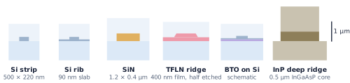
TFLN has no detectors or gain of its own, and lithium is not welcome in CMOS fabs, so the material is processed in dedicated lines. Luxtelligence and HyperLight are among the foundries; Luxtelligence’s PDK is open, and three of its devices appear in the 3D gallery [21]. Its typical waveguide is etched halfway into the film, so the ridge sits on a thin slab (Figure 4.2).
4.6Barium titanate
Barium titanate (BaTiO₃, BTO) is a ferroelectric perovskite with one of the largest known Pockels coefficients. Grown as an epitaxial film on silicon, it retains effective coefficients of hundreds of picometres per volt [33], an order of magnitude more than lithium niobate. Because the film can be deposited on silicon wafers, BTO promises Pockels modulators and phase shifters inside a silicon-photonics process, with very low static power, which matters for large switching and computing meshes where thousands of thermal phase shifters would otherwise burn watts.
The integration is demanding: the film must be grown on a template layer and bonded, its crystal domains must be oriented for the field direction of the electrodes, and the effective coefficient depends on frequency and processing. Typical devices place a silicon or silicon nitride waveguide on or under a thin BTO film, so that part of the mode sees the BTO. BTO is earlier in its industrial development than the other platforms here, and no open PDK exists yet.
4.7Indium phosphide and other III–Vs
Indium phosphide and the alloys lattice-matched to it, InGaAsP and InGaAlAs, have direct bandgaps that can be tuned across the telecom bands. A single InP wafer can therefore carry lasers, semiconductor optical amplifiers, electro-absorption and Mach–Zehnder modulators, photodetectors and passive waveguides, all monolithically integrated [4]. Generic InP foundry platforms, such as those at Fraunhofer HHI and SMART Photonics, offer these through MPW runs.
The price is in the passive parts. The vertical index contrast between an InGaAsP core and InP cladding is small, so waveguides are wide and deeply etched, bends are tens to hundreds of micrometres, propagation losses are a few dB/cm, and the substrates are small (75–100 mm) and expensive. This is why the dominant approach for high-volume products combines InP gain with silicon or silicon nitride circuits, by attaching, bonding or growing III–V material on silicon (Chapter 27). Gallium arsenide plays the same role for quantum-dot lasers near 1310 nm and for shorter wavelengths, and germanium is the detector material of silicon photonics.
4.8Choosing and combining platforms
Figure 4.2 draws typical waveguides of each platform at the same scale. The silicon strip is the smallest by far; the InP ridge is the largest, because its low vertical contrast forces a thick core.
figsrc/part1_figs.py.Try it. Compare any two platforms: their cross-sections, typical loss and bend radius, index contrast and native capabilities.
When no single platform does everything, the chip combines them. The vocabulary is worth fixing early:
- Monolithic integration builds every function in one material and process: an InP PIC with lasers, or a silicon PIC with germanium detectors.
- Hybrid integration assembles finished chips: a laser die flip-chipped or butt-coupled to a silicon chip, or attached through micro-optics.
- Heterogeneous integration bonds unprocessed material, such as an InP die or wafer, onto a patterned silicon wafer and then processes it there with wafer-scale lithography, so that the III–V devices are aligned to the silicon circuits lithographically [34].
- Micro-transfer printing sits between the two: finished micro-devices are picked from their source wafer and printed onto the target wafer in parallel.
Chapter 27 compares these for lasers. Silicon nitride layers in silicon processes, TFLN bonded onto silicon, and BTO grown on silicon are all heterogeneous combinations of the same kind.
Open PDKs used in this tutorial
Process design kits (Chapter 30) are usually under non-disclosure agreements. A few are open source, and this tutorial uses only those for its layouts, labs and 3D models.
Table 4.3. Open photonic PDKs used in this tutorial. All MIT-licensed; see Appendix D for links.
| PDK | Platform | Used for |
|---|---|---|
| SiEPIC EBeam PDK [15] and its gdsfactory version, ubcpdk [18] | 220 nm SOI (and SiN), electron-beam lithography, openEBL runs | the labs’ first chip, 3D models, measured data |
| CORNERSTONE, via cspdk [19] | 220 and 340 nm SOI, SiN, Ge-on-Si | 3D models, cross-platform comparisons |
| Luxtelligence LNOI400, via lnoi400 [21] | thin-film lithium niobate | 3D models, modulator examples |
| VTT, via gvtt [20] | 3 µm thick SOI | thick-SOI examples |
Choose the platform from the function that is hardest to get. If you need density and volume, start in silicon and bring in the laser. If you need the lowest loss or visible wavelengths, SiN. If you need the fastest, most linear modulator, TFLN, or BTO where it is available. If you need gain everywhere, InP. For the reference link, silicon carries the modulators, filters and detectors, and the laser comes from III–V material (Chapter 27).
Silicon photonics in 220 nm SOI, with germanium photodetectors, carrier-depletion ring modulators and metal heaters, and four III–V lasers brought in from outside the silicon. The passive devices of the labs’ first chip use the same 220 nm platform.
Reading
- [29] Shawn Yohanes Siew et al. “Review of silicon photonics technology and platform development.” Journal of Lightwave Technology, 39(13):4374–4389, 2021. Open access.
- [31] Daniel J. Blumenthal, René Heideman, Douwe Geuzebroek, Arne Leinse and Chris Roeloffzen. “Silicon nitride in silicon photonics.” Proceedings of the IEEE, 106(12):2209–2231, 2018. Open access.
- [32] Di Zhu et al. “Integrated photonics on thin-film lithium niobate.” Advances in Optics and Photonics, 13(2):242–352, 2021.
- [33] Stefan Abel et al. “Large Pockels effect in micro- and nanostructured barium titanate integrated on silicon.” Nature Materials, 18:42–47, 2019.
- [34] Tin Komljenovic et al. “Heterogeneous silicon photonic integrated circuits.” Journal of Lightwave Technology, 34(1):20–35, 2016.
- [28] Sudip Shekhar, Wim Bogaerts, Lukas Chrostowski, John E. Bowers, Michael Hochberg, Richard Soref and Bhavin J. Shastri. “Roadmapping the next generation of silicon photonics.” Nature Communications, 15:751, 2024. Open access.
- [4] Larry A. Coldren, Scott W. Corzine and Milan L. Mašanović. Diode Lasers and Photonic Integrated Circuits, 2nd edition. Wiley, 2012.
- A platform must guide, tune, modulate, detect, generate and amplify light; none does all six natively.
- Silicon: highest contrast and CMOS volume, no laser or Pockels effect. SiN: lowest loss and widest transparency, no fast modulation or detection. TFLN and BTO: strong Pockels modulation. InP: everything including gain, with larger, lossier passives on small wafers.
- The bandgap sets the short-wavelength transparency edge, \(\lambda_g = 1.24/E_g\) µm; germanium’s direct gap at 0.80 eV puts its edge at the C band.
- Monolithic, hybrid, heterogeneous and transfer-printed integration combine platforms; most modern transceivers are silicon with attached or bonded III–V lasers.
- This tutorial uses only open PDKs: SiEPIC EBeam, CORNERSTONE, Luxtelligence and VTT.