Chapter 2Electromagnetic Theory for Photonics
Every device in this tutorial is a solution of Maxwell’s equations for a particular arrangement of refractive index.
- write Maxwell’s equations for a source-free dielectric and derive the wave equation;
- describe a plane wave by its wavevector, frequency, wavelength, index and impedance;
- relate permittivity to the complex refractive index, absorption and material dispersion;
- describe polarisation and the power a wave carries;
- compute Fresnel reflection, Brewster’s angle, the critical angle and the evanescent decay length;
- distinguish phase velocity from group velocity and compute the group index.
What does light do at an interface between two materials, and how does that lead to confinement in a waveguide?
2.1Maxwell’s equations in matter
Light is an electromagnetic wave, described by the electric field \(\mathbf{E}\), the magnetic field \(\mathbf{H}\), the electric displacement \(\mathbf{D}\) and the magnetic flux density \(\mathbf{B}\). In a material with no free charges or currents, which covers every waveguide core and cladding in this tutorial, Maxwell’s equations read
The material enters through the constitutive relations. Photonic materials are not magnetic, so \(\mathbf{B} = \mu_0\mathbf{H}\). In a linear, isotropic dielectric the displacement is proportional to the field, \(\mathbf{D} = \varepsilon_0\varepsilon_r\mathbf{E}\), with the relative permittivity \(\varepsilon_r = n^2\). Silicon, silica, silicon nitride and indium phosphide are isotropic to a good approximation. Lithium niobate and barium titanate are not: their permittivity is a tensor that depends on the direction of the field relative to the crystal axes, and an applied voltage changes it, which is the Pockels effect of Chapter 19.
We write time-harmonic fields with the engineering convention
\[\mathbf{E}(\mathbf{r},t) = \mathrm{Re}\left\{\mathbf{E}(\mathbf{r})\,e^{j\omega t}\right\},\]so that \(\partial/\partial t \to j\omega\) and a wave travelling in \(+z\) varies as \(e^{j(\omega t - \beta z)}\). Physics texts and several simulation tools use \(e^{-i\omega t}\) instead, which flips the sign of every imaginary part (a lossy index becomes \(n + i\kappa\) instead of \(n - j\kappa\)). Neither is wrong; mixing them is.
2.2The wave equation and plane waves
Taking the curl of Faraday’s law and substituting Ampère’s law gives, in a homogeneous medium,
\[\nabla^2\mathbf{E} - \mu_0\varepsilon_0 n^2\frac{\partial^2\mathbf{E}}{\partial t^2} = 0 \quad\Longrightarrow\quad \nabla^2\mathbf{E} + n^2 k_0^2\,\mathbf{E} = 0,\]the Helmholtz equation, with the vacuum wavenumber \(k_0 = \omega/c = 2\pi/\lambda_0\) and \(c = 1/\sqrt{\mu_0\varepsilon_0}\). Its simplest solution is the plane wave \(\mathbf{E} = \mathbf{E}_0\,e^{j(\omega t - \mathbf{k}\cdot\mathbf{r})}\) with \(\lvert \mathbf{k}\rvert = nk_0\). The field is transverse (\(\mathbf{k}\cdot\mathbf{E}_0 = 0\)), the magnetic field is \(\mathbf{H} = \hat{\mathbf{k}}\times\mathbf{E}/\eta\), and the ratio of the two is the wave impedance \(\eta = \eta_0/n\) with \(\eta_0 = \sqrt{\mu_0/\varepsilon_0} \approx 376.7\ \Omega\).
Inside the material the wavelength shrinks to \(\lambda = \lambda_0/n\) and the crests travel at the phase velocity \(v_p = c/n\). The frequency does not change at an interface; the wavelength does.
Light at \(\lambda_0 = 1550\) nm has a frequency \(f = c/\lambda_0 = 193.4\) THz and a photon energy \(hc/\lambda_0 = 1.2398/1.55 = 0.800\) eV. In silicon (\(n = 3.476\)) its wavelength is \(1550/3.476 = 446\) nm, which is why silicon waveguides are a few hundred nanometres across. Differentiating \(f = c/\lambda\) gives \(\lvert \Delta f\rvert = c\,\Delta\lambda/\lambda^2\): near 1550 nm, 1 nm of wavelength is 124.8 GHz, so a 0.8 nm (100 GHz) WDM grid and a 3.2 nm (400 GHz) grid are the same thing in two units.
2.3Refractive index, absorption and dispersion
Complex index and loss
A material that absorbs has a complex permittivity, and therefore a complex index \(\tilde n = n - j\kappa\) (in our convention). A plane wave then varies as \(e^{-jk_0(n - j\kappa)z} = e^{-jk_0nz}\,e^{-k_0\kappa z}\): the field decays as \(e^{-k_0\kappa z}\) and the power as \(e^{-\alpha z}\), with the power absorption coefficient
A waveguide loss of 2 dB/cm is therefore \(\alpha = 2/4.343 = 0.46\ \mathrm{cm^{-1}}\), and corresponds to an extinction coefficient of only \(\kappa = \alpha\lambda_0/4\pi \approx 5.7\times10^{-6}\): tiny imaginary parts matter over centimetres. In a waveguide most of the loss comes from scattering and from light leaking into the substrate rather than from absorption in the material (Chapter 7), but it is still described by an α.
Material dispersion
The index depends on wavelength, because the electrons and ions of a material respond more strongly near their resonances. Far from the resonances this is captured by a Sellmeier model, a sum of a few oscillator terms:
\[n^2(\lambda) = 1 + \sum_i \frac{B_i\lambda^2}{\lambda^2 - C_i},\]with coefficients fitted to measurements. Figure 2.1 plots published models for silicon [59], silica [58], LPCVD silicon nitride [60] and lithium niobate [61], and Table 2.1 gives their values at the two telecom bands.
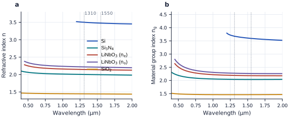
figsrc/part1_figs.py.Table 2.1. Refractive index and material group index. From the Sellmeier models of Figure 2.1.
| Material | n at 1310 nm | n at 1550 nm | n_g at 1550 nm |
|---|---|---|---|
| Silicon | 3.501 | 3.476 | 3.59 |
| Silicon nitride (LPCVD) | 2.003 | 1.996 | 2.04 |
| Lithium niobate, extraordinary | 2.145 | 2.138 | 2.18 |
| Lithium niobate, ordinary | 2.220 | 2.211 | 2.26 |
| Silica | 1.447 | 1.444 | 1.46 |
The index also changes with temperature. Silicon’s thermo-optic coefficient, \(\mathrm{d}n/\mathrm{d}T \approx 1.8\times10^{-4}\ \mathrm{K^{-1}}\) at 1550 nm, is roughly ten times that of silica or silicon nitride. It is a gift for tuning (Chapter 18) and a curse for stability.
2.4Polarisation and power
The direction of the electric field is the polarisation. For a plane wave travelling along \(z\), the field is the sum of two components,
\[\mathbf{E}(t) = \hat{\mathbf{x}}\,E_x\cos\omega t + \hat{\mathbf{y}}\,E_y\cos(\omega t + \delta),\]and the tip of \(\mathbf{E}\) traces a line if the components are in phase (\(\delta = 0\) or \(\pi\)), a circle if they are equal and a quarter-period apart (\(\lvert E_x\rvert = \lvert E_y\rvert\), \(\delta = \pm\pi/2\)), and an ellipse otherwise. Written as a Jones vector, \([E_x,\ E_y e^{j\delta}]\), any polarisation is a pair of complex numbers, and a polarising element is a 2 × 2 matrix acting on it.
Try it. Add two components with any amplitude and phase and watch the polarisation ellipse.
Waveguides on a chip are strongly polarisation-dependent: a silicon strip guides a mode with the field mostly in the plane of the chip (TE-like) and another with the field mostly normal to it (TM-like), with different effective indices, losses and coupling. Standard single-mode fibre, in contrast, scrambles the polarisation as it bends and warms. The meeting of the two is the subject of Chapter 14.
The power carried by the wave flows along the Poynting vector \(\mathbf{S} = \mathbf{E}\times\mathbf{H}\). For time-harmonic fields its average is \(\langle\mathbf{S}\rangle = \tfrac12\mathrm{Re}\{\mathbf{E}\times\mathbf{H}^*\}\), and for a plane wave the intensity is
\[I = \frac{\lvert E_0\rvert ^2}{2\eta} = \frac{n\,\lvert E_0\rvert ^2}{2\eta_0}.\]A silicon strip waveguide squeezes its mode into roughly 0.1 µm². One milliwatt in that area is an intensity of \(10^{-3}/10^{-13} = 10^{10}\ \mathrm{W/m^2}\), or 1 MW/cm². The peak field is \(\lvert E_0\rvert = \sqrt{2\eta_0 I/n} = \sqrt{2\times376.7\times10^{10}/3.48} \approx 1.5\) MV/m. Intensities like this are why nonlinear effects such as two-photon absorption appear in silicon at only tens of milliwatts (Chapter 7), and why a laser that is gentle in a fibre is not gentle in a nanowire.
2.5Reflection and refraction
At a flat interface between media of index \(n_1\) and \(n_2\), the tangential components of \(\mathbf{E}\) and \(\mathbf{H}\) must be continuous. Matching the phase of the incident, reflected and transmitted waves along the interface gives Snell’s law,
\[n_1\sin\theta_1 = n_2\sin\theta_2,\]and matching their amplitudes gives the Fresnel coefficients. They differ for the two polarisations: s (electric field perpendicular to the plane of incidence, also called TE) and p (in the plane, TM). With \(\cos\theta_2 = \sqrt{1 - (n_1/n_2)^2\sin^2\theta_1}\),
At normal incidence both reduce to \(R = \left[(n_1 - n_2)/(n_1 + n_2)\right]^2\). The p reflection vanishes at Brewster’s angle, \(\tan\theta_B = n_2/n_1\).
A cleaved silicon facet in air reflects \(R = (2.476/4.476)^2 = 30.6\ \%\) of the light at normal incidence. Against silica it reflects \((2.032/4.920)^2 = 17.1\ \%\), silicon nitride against silica only \((0.552/3.440)^2 = 2.6\ \%\), and lithium niobate (extraordinary) against silica \(3.8\ \%\). Two parallel silicon facets form a Fabry–Pérot cavity, and the 30 % mirrors of an InP laser are exactly such cleaved facets (Chapter 24).
Any abrupt change of index reflects. In a measurement, reflections at the two ends of a chip form a cavity whose fringes ripple across the spectrum and can be mistaken for device features (Chapter 31); light reflected back into a laser can destabilise it (Chapter 25). Tapers, angled facets and anti-reflection coatings exist to remove them (Chapter 16).
2.6Total internal reflection and evanescent waves
When light goes from a high index to a low one, Snell’s law has no real solution beyond the critical angle
\[\sin\theta_c = \frac{n_2}{n_1},\]and all the power is reflected. The field does not stop at the interface, though. Its component of the wavevector along the interface is \(\beta = n_1k_0\sin\theta_1\), and the wave equation in medium 2 then requires a normal component \(k_x^2 = n_2^2k_0^2 - \beta^2\), which is negative beyond \(\theta_c\). The field in medium 2 therefore decays exponentially away from the interface instead of propagating: it is an evanescent wave,
where we have written \(n_1\sin\theta_1\) as \(n_\mathrm{eff}\). That name is deliberate: a guided mode is light bouncing between two interfaces beyond the critical angle, and its effective index is exactly \(n_1\sin\theta_1\) (Chapter 5). The reflected wave also picks up a phase shift that depends on angle and polarisation, and appears displaced along the interface (the Goos–Hänchen shift), as if it had penetrated a distance of order \(1/\gamma\) before turning back.
Try it. Increase the angle past the critical angle and watch the transmitted ray vanish and the evanescent tail appear.
The critical angle between silicon and silica is \(\arcsin(1.444/3.476) = 24.5°\), against air 16.7°, and between silicon nitride and silica 46.3°: the lower the contrast, the more grazing the light must be to stay confined. A 220 nm silicon slab guides its fundamental TE mode with \(n_\mathrm{eff} \approx 2.85\) (Chapter 5), which corresponds to rays at \(\arcsin(2.85/3.476) = 55°\). Its field decays into the oxide with
\[\gamma = \frac{2\pi}{1.55\ \mu\mathrm{m}}\sqrt{2.848^2 - 1.444^2} = 9.95\ \mu\mathrm{m}^{-1}, \qquad 1/\gamma \approx 100\ \mathrm{nm}.\]The intensity falls by \(e\) in only 50 nm.
In silicon photonics the evanescent field reaches about 100 nm into the cladding. Everything that interacts with a guided mode from outside does so through this tail: two waveguides couple when their gap is a few times \(1/\gamma\), so directional couplers use gaps of 100–300 nm (Chapter 9); sidewall roughness scatters light from it (Chapter 7); and a biosensor sees only molecules within it (Chapter 34). Lower-contrast platforms such as silicon nitride have longer tails, so their gaps and bends are larger.
2.7Phase velocity, group velocity and group index
A single frequency carries no information; a signal is a packet of frequencies. Two waves at \(\omega\pm\Delta\omega\) with wavenumbers \(\beta\pm\Delta\beta\) add to a carrier at \(\omega\) under an envelope \(\cos(\Delta\omega\,t - \Delta\beta\,z)\), which moves at \(\Delta\omega/\Delta\beta\). In the limit this is the group velocity \(v_g = \mathrm{d}\omega/\mathrm{d}\beta\), the speed of the envelope and therefore of energy and information. With \(\beta = n\omega/c\),
\[\frac{1}{v_g} = \frac{\mathrm{d}\beta}{\mathrm{d}\omega} = \frac{1}{c}\left(n + \omega\frac{\mathrm{d}n}{\mathrm{d}\omega}\right),\]and since \(\omega\,\mathrm{d}n/\mathrm{d}\omega = -\lambda\,\mathrm{d}n/\mathrm{d}\lambda\):
The same formula holds for a waveguide mode with \(n\) replaced by \(n_\mathrm{eff}\), and there the waveguide’s own dispersion adds to the material’s. Silicon’s material group index is 3.59 at 1550 nm, but a 500 × 220 nm silicon waveguide has \(n_\mathrm{eff} \approx 2.4\) and \(n_g \approx 4.2\): its effective index falls quickly with wavelength because a longer wavelength pushes more of the mode into the cladding (Chapter 6). The group index sets the time of flight, \(\tau = n_gL/c\) (140 ps for 1 cm of silicon wire), and, as later chapters show, the free spectral range of every interferometer and resonator.
Try it. Set the phase and group index and watch the crests slide through the envelope.
When the group velocity itself depends on frequency, different parts of a pulse’s spectrum arrive at different times and the pulse spreads. This group-velocity dispersion is written \(\beta_2 = \mathrm{d}^2\beta/\mathrm{d}\omega^2\), or for fibres as the dispersion parameter \(D = -(2\pi c/\lambda^2)\beta_2\) in ps/(nm·km). Standard single-mode fibre has \(D \approx 17\) ps/(nm·km) at 1550 nm and crosses zero near 1310 nm [57].
Two kilometres of standard fibre at 1550 nm accumulate \(17\times2 = 34\) ps/nm of dispersion. A 50 Gb/s NRZ signal occupies roughly 50 GHz, or 0.4 nm, so its spectral components spread by about \(34\times0.4 \approx 14\) ps, a large fraction of the 20 ps bit. A rule of thumb from 10 Gb/s systems, where chirp-free NRZ tolerates roughly 1000–1600 ps/nm, scales as \(1/B^2\) to about 40–60 ps/nm at 50 Gb/s: the reference link is inside the limit, but not by much, and a modulator’s chirp eats into it. This is one reason data-centre links often use the O band, where the fibre’s dispersion is near zero. Chapter 33 puts the penalty into the budget.
Free simulations by others that pair well with this chapter:
Reading
- [2] Bahaa E. A. Saleh and Malvin C. Teich. Fundamentals of Photonics, 3rd edition. Wiley, 2019.
- [6] Amnon Yariv and Pochi Yeh. Photonics: Optical Electronics in Modern Communications, 6th edition. Oxford University Press, 2007.
- [1] Lukas Chrostowski and Michael Hochberg. Silicon Photonics Design: From Devices to Systems. Cambridge University Press, 2015. https://www.cambridge.org/core/books/silicon-photonics-design/BF3CF13E8542BCE67FD2BBC7104ECEAB
- [59] H. H. Li. “Refractive index of silicon and germanium and its wavelength and temperature derivatives.” Journal of Physical and Chemical Reference Data, 9(3):561–658, 1980.
- [58] I. H. Malitson. “Interspecimen comparison of the refractive index of fused silica.” Journal of the Optical Society of America, 55(10):1205–1209, 1965.
- [60] Kevin Luke, Yoshitomo Okawachi, Michael R. E. Lamont, Alexander L. Gaeta and Michal Lipson. “Broadband mid-infrared frequency comb generation in a Si₃N₄ microresonator.” Optics Letters, 40(21):4823–4826, 2015.
- [61] David E. Zelmon, David L. Small and Dieter Jundt. “Infrared corrected Sellmeier coefficients for congruently grown lithium niobate and 5 mol.% magnesium oxide-doped lithium niobate.” Journal of the Optical Society of America B, 14(12):3319–3322, 1997.
- Light obeys the Helmholtz equation \(\nabla^2\mathbf{E} + n^2k_0^2\mathbf{E} = 0\); in a material its wavelength is \(\lambda_0/n\) and its impedance \(\eta_0/n\). At 1550 nm, 1 nm of wavelength is about 125 GHz.
- Loss is the imaginary part of the index: \(\alpha = 4\pi\kappa/\lambda_0\), and \(\alpha_\mathrm{dB} = 4.343\,\alpha\).
- Silicon’s index is 3.476 at 1550 nm, silica’s 1.444, silicon nitride’s about 2.0; silicon’s thermo-optic coefficient is about ten times that of the other two.
- Beyond the critical angle all power is reflected, but an evanescent field reaches about \(1/\gamma\) into the low-index side: about 100 nm in silicon photonics. Couplers, sensors and scattering losses all work through it.
- Energy and information travel at the group velocity, \(n_g = n - \lambda\,\mathrm{d}n/\mathrm{d}\lambda\); for a silicon wire \(n_g \approx 4.2\), well above \(n_\mathrm{eff} \approx 2.4\).